Objective: By the end of this lecture, the student should be able to edit the model parameter of a NMOS and use a piecewise linear model, PWL, to compare the ideal with the experimental values.
Sec. 8.1 NMOS parameter
ĀĀĀĀĀĀĀĀĀĀĀ PSpice contain a lot of models for specific element, but not all the elements that exist in the world.Ā For this part of the lecture, a NMOS model will be modified to reflect the measured parameters of an actual NMOS.Ā For this exercise, we will be using the figure shown in fig. 8-1.Ā This circuit is a NMOS inverter.Ā
- Create the circuit as shown in fig. 8-1.

Fig. 8-1 – NMOS inverter
- The NMOS is in the Breakout library
- The Breakout library is design for user to create user-defined models.
- 7Select the NMOS and click Edit/PSpice Model
- Once the Model Editor window opens, type in the values as
shown in Appendix VI
*NOTE – These are the parameters I measured in the lab for a ECG4007* - Save the model with the default name
- Close the program
- Create a triangular wave with a amplitude of 8V @ 60 Hz
- Create a transient analysis
- Simulate the circuit.
- In the Probe window, change the x-axis to point at the input voltage source.
- In the Probe window, click on Plot/Axis Setting
- In the Axis Setting dialog box, click on Axis Variable,
refer to fig. 8-2
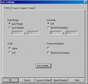
Fig. 8-2 – Axis Setting dialog box
- In the X Axis Variable dialog box, type in the expression
v(in), refer to fig. 8-3
*Type in v(in) only if you label the node, else, type in or select the input voltage
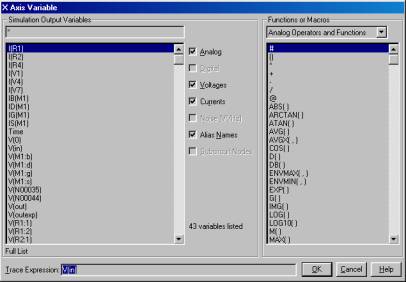
Fig. 8-3 – Axis Variable dialog box
- Click OK
- Click OK
- In the Capture window, place a voltage marker at the drain of the NMOS
- The VTC should be similar to fig. 8-4
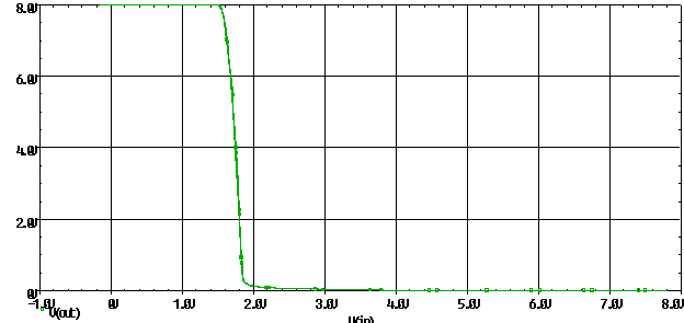
Fig. 8.4 – VTC of NMOS inverter
Sec. 8.2 Using experimental data
ĀĀĀĀĀĀĀĀĀĀĀ PSpice is a great way to see the ideal values of a circuit, but it would be real nice if PSpice could display the ideal and experimental values at the same time.Ā And surprisingly, it is possible, but to a certain extend.Ā To do the following simulation, you would need to download two files first.Ā The files can be obtained at http://www.tinmancp.com/spice/.Ā The two files are call vin_10k_small.csv and vout_10k_small.csv.Ā As the name of the files implied, one is a input signal and the other is the output signal.Ā The file vin_10k_small.csv contains a triangular wave and the file vout_10k_small.csv contain the output waveform at the drain of the NMOS.
- Use the same circuit shown in fig. 8-1.
- Instead of using a voltage source at the input, put a piecewise linear source, refer to fig. 8.5.
- The PWL is located in the source library
- The specific part is call VPWL_FILE
This part used a data file as the input. - Change the value of the PWL to vin_10k_small.csv
- Create another circuit with PWL in series with a resistor, refer
to fig. 8-5
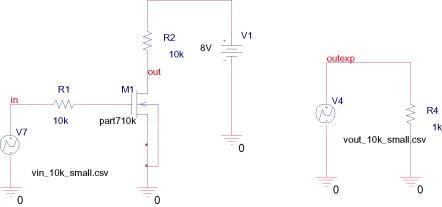
Fig. 8-5 – NMOS inverter with PWL
- Change the value of the PWL to vout_10k_small.csv, refer to fig. 8-5
- I like to label the output so it would be easier to identify which output is which
- Create a new simulation profile
- Select transient analysis as the analysis type.
- Choose a run time of 50ms.
- Simulate the circuit.
- Change the axis setting to show the input voltage
Sec. 8.3 creating a VTC
ĀĀĀĀĀĀĀĀĀĀĀ Since we are doing a transient analysis, the x-axis would show the time scale.Ā What we want is a VTC, which is by definition a graph of the output vs. the input.Ā To create the VTC with a transient analysis, follow the following step.Ā I am assuming that you have simulated the circuit.
- In the Probe window, click on Plot/Axis Setting
- In the Axis Setting dialog box, click on Axis Variable
- In the X Axis Variable dialog box, type in the expression
v(in)
*Type in v(in) only if you label the node, else, type in or select the input voltage - Click OK
- Click OK
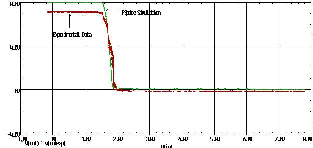
- In the Probe window, add a trace for the output from the spice simulation and a trace for the output from the experimental data.Ā Conversely, place two voltage markers in the Capture window, one on the output node of the circuit and the other on the output for the PWL.Ā The figure should look like fig. 8.6
|
|
|
Fig 8-6 – VTC from PSpice and experimental data |
.model 453nmos NMOS

+ Level=1

+ VTO=1.5164

+ KP=0.00136242

+ GAMMA=0.95142

+ PHI=0.65

+ LAMBDA=0.00907

+ RD=1.0

+ RS=1.0

+ CBD=2.0E-14

+ CBS=2.0E-14

+ IS=1.0E-15

+ PB=0.87

+ CGSO=4.0E-11

+ CGDO=4.0E-11

+ CGBO=2.0E-10

+ RSH=10.0

+ CJ=2.0E-4

+ MJ=0.5

+ CJSW=1.0E-9

+ JS=1.0E-8

+ TOX=1.0E-7

+ NSUB=4.0E15

+ NSS=1.0E10

+ NFS=1.0E-10

+ XJ=1.0E-6

+ LD=0.8E-6

+ UO=580