Objective:
ааааааааааа By the end of this lecture, students will be able to perform a DC Sweep and Transient analysis using PSpice.а Time permitting, students will also learn how to create a SPICE file to perform the analysis.
Sec. 2.1 Preparing the schematic
- Follow a procedure similar to lecture 1 to create a new project.
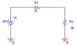
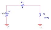
- Draw the circuit as shown in fig. 2-1. (All the steps are similar to those illustrated in lecture 1)
|
|
| Fig. 2-1 – Circuit used for DC Sweep |
Sec. 2.2 How to setup DC Sweep analysis
- Click on PSpice/New Simulation Profile.а
- Type in DC Sweep for the Name field
- Select none in the Inherit From field
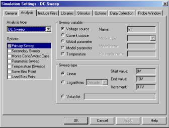
- In the Simulation Setting dialog box select the following (refer to fig. 2-2)
- In the Analysis Type field, select DC Sweep
- In the Name field, type in v1 or the name of the source that is to be sweep
- Select Voltage Source since we are sweeping the voltage source
- Select linear for the Sweep type
- Type in 0V for the Start Value, 10V for the End Value, and 0.1V for the Increment
- Click OK
|
|
| Fig. 2-2 – Simulation Setting dialog box |
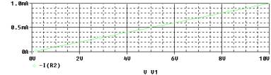
Sec. 2.3 Working in the Probe window (Proving resistors are linear element)
ааааааааааа We will determine if R2 is a linear element.а From our study of basic circuits, we are told that voltage varies linearly with current.а The equation to predict the voltage through the resistor is V=RI.а Using the Probe facility, we will show this graphically by plotting the i-v curve of R2.
- Run the simulation by clicking PSpice/Run.
- In the Probe window, click on Trace/Add Trace to access the Add Trace window (refer to fig. 2-3).
|
|
| Fig. 2-3 – Add Traces dialog box. |
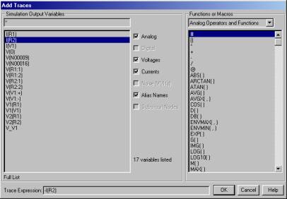
- In the Trace Expression field, type in –I(R2).
- Click OK
- Alternately, we can also add the trace in the Capture window.
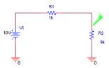
- In the Capture window, click on PSpice/Markers/Current Marker.
- In the schematic, place the marker on the pin of R2 (refer
to fig. 2-4).
- Go to the Probe window and a trace should automatically appear
|
|
| Fig. 2-4 – How to place the current marker |
- Your graph should look like fig. 2-5.
|
|
| Fig. 2-5 – The plot to showing DC Sweep |
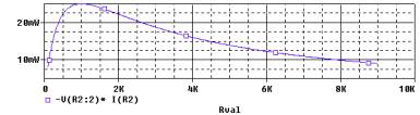
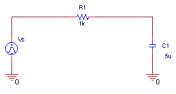
Sec. 2.4 Determining the maximum power transfer
To generate a graph of power versus R2, we will be sweeping R2 through a range of values.а To do this we will be setting up a global parametric sweep.
- Go to the schematic and change the value of R2 from 9k to {rval} (refer to fig. 2-6).
|
|
| Fig. 2-6 – Modified schematic for parametric sweep |
- Click on Place/Part to access the Get New Part dialog box
- In the Get New Part dialog box, do the following
- In the Libraries area, select SPECIAL
- In the Part area, type in PARAM or scroll down until you see PARAM
- Click OK
- Double click the PARAM part to display the Parts Spreadsheet.
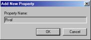
- Click New to access the Add New Property dialog box (refer to fig. 2-7).
|
|
| Fig. 2-7 – Add New Property dialog box |
- Type in Rval
- Click OK
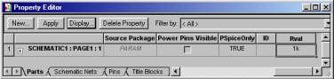
- This will create a new property for the PARAM part (refer to fig. 2-8).
|
|
| Fig. 2-8 – Parts spreadsheet |
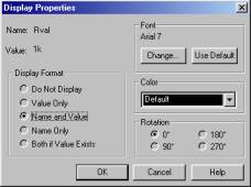
- In the cell below the Rval column, type in 1k
- With the cell still selected, click on Display to access the Display Properties dialog box.
- In the Display Format dialog box, select Name and Value (refer to fig. 2-9).
|
|
| Fig. 2-9 – Display Properties dialog box |
- Click OK
- Click Apply
- Close Parts window.
- Click on PSpice/New Simulation Profile, to access New Simulation
Profile dialog box.
- In the Name field, type in Parametric
- In the Inherit From field, select None
- Click CREATE
- In the Simulation Settings dialog box, do the following (refer
to Fig. 2-10).

Fig. 2-10 – Simulation Settings for parametric sweep. - In the Analysis Type field, select DC Sweep.
- In the Options filed, leave the default setting.
- In the Sweep Variable area, select Global Parameter.
- In the Parameter Name area, type in Rval
- Select Linear Type in the Sweep type area.
- Type in 100 for the Start Value, 9k for the End Value, and 10 for the increment
- Click OK
- Click on PSpice/Run
- In the Probe window, click on Trace/Add Traces
- In the Trace Expression field, type in -V(R2:2)* I(R2)
- Click OK
- Your graph should be similar to fig 2-11.
|
|
| Fig. 2-11 – Maximum power transfer curve |
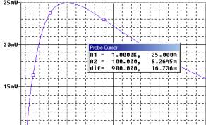
Sec. 2.5 Using the cursor tool
- Click on Trace/Cursor/Display, this will active the cursor.а A crosshair should appear on the graph.
- Click and drag the crosshair until you reach the peak of the graph.
- Look at the Probe Cursor box to determine the values (refer to fig. 2-12).
- From the box, the value for the x-axis is 1k
- From the box, the value for the y-axis is 25mW
|
|
| Fig. 2-12 – Probe cursor box |
Sec. 2.6 Simple RC circuit
ааааааааааа The RC circuit shown in fig 2-13 is the first circuit most of us are exposed to when we are introduced to a first order system.а Using PSpice, we will see how the capacitor charges and discharges when the voltage source is a pulse wave.
|
|
| Fig. 2-13 – Simple RC circuit |
- Create a new project.
- Get and place the parts.
- The value for R1 is 1kW.
- The value for C1 is 1mF
- The pulse wave is call VPULSE and is located in the SOURCE library.
- To change the value of the pulse, double click on it to access the property datasheet.
- In the datasheet, enter the following values
- TD = 0а (Time Delay)
- TF = 0.01msа (Fall Time)
- TR = 0.01msа (Rise Time)
- PW = 5msа (Pulse Width)
- PER = 10msа (Period)
- V1 = 0V (Voltage Minimum)
- V2 = 5V (Voltage Maximum)
- Reference = Vs (Name of the Voltage Source)
This setting will create a pulse with an amplitude of 5V and a frequency of 100 Hz.
- Create a new Simulation Profile
- Select Transient Analysis for the analysis type.
- Type in 30ms for the Run to Time
- Type in 1ms for the Maximum Step Size
- The step size tells PSpice to output the results at a 1ms interval
- Click OK
- Run the simulation
- In the Probe Window, add traces to show the pulse wave and the voltage drop across the capacitor.
- To show the pulse wave, add the trace expression V(Vs:+).
- To show the voltage drop across the capacitor, add the trace expression V(c1:2)
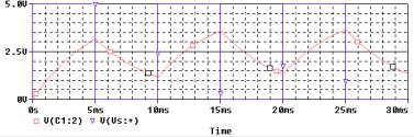
Sec 2.7 Interpreting the results for the RC circuit
ааааааааааа From the probe result, we can see that the capacitors charges during the positive cycle of the pulse and discharges during the zero portion of the pulse.а The capacitor doesn’t fully discharges because of the time constant is longer than the pulse period.
|
|
| Fig. 2-14 – Transient response of a RC circuit |
Sec. 2.8 Getting values to export to other applications
ааааааааааа PSpice does a very good job at plotting waveforms and helping us interpret results.а But with every application, there are limitation to what it can do.а Using the RC circuit as an example, let say there are some additional analysis that you wish to perform but PSpice does not have the capability to do it.а Then the best way to do this is to a combination of the .PRINT and output file options.а
- Using the same circuit of the RC circuit, fig.2.13, add a .PRINT
parts to the circuit, refer to fig. 2-15.
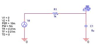
Fig. 2-15 – RC circuit with PRINT1 part - The .PRINT part is located in the Special library and is call PRINT1
- Click on PSpice/Edit Simulation Settings.
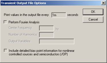
- In the Simulation Settings dialog box, click on Output File Options.а The Transient Output File Options should appear, refer to fig. 2-16.
- In the Print values in the output file every field, type in 1ms.а This would tell PSpice to print the output every 1ms.
- Click OK.
- Click OK.
- Run the simualation.
|
|
| Fig. 2-16 – Output file options dialog box |
Sec. 2.8 Getting the results
ааааааааааа Once the simulation is run, you would still have the same graph as the first time the simulation was run.а To view the output, go to the Probe window and click on View/Output file.а Scroll down until you see the results.а To see the complete output file, refer to Appendix IV.а The result can now be imported to other application to perform additional analysis.
**** 03/06/00 00:15:01 ********* PSpice 9.0 (Nov 1998) ******** ID# 0 ******** ** circuit file for profile: fig13 ****аааа CIRCUIT DESCRIPTION ****************************************************************************** ** WARNING: DO NOT EDIT OR DELETE THIS FILE *Libraries: * Local Libraries : * From [PSPICE NETLIST] section of pspice.ini file: .lib "nom.lib" *Analysis directives: .TRAN 1m 30m 0 1m .PROBE *Netlist File: .INC "fig12-SCHEMATIC1.net" *Alias File: **** INCLUDING fig12-SCHEMATIC1.net **** * source FIG12 C_C1аааааааа 0 N00034а 5uа R_R1аааааааа N00027 N00034а 1k V_Vsаааааааа N00027 0 +PULSE 0 5 0 0.01m 0.01m 5m 10m .PRINTаааааааа TRAN V([N00034]) **** RESUMING fig12-schematic1-fig13.sim.cir **** .INC "fig12-SCHEMATIC1.als" **** INCLUDING fig12-SCHEMATIC1.als **** .ALIASES C_C1ааааааааааа C1(1=0 2=N00034 ) R_R1ааааааааааа R1(1=N00027 2=N00034 ) V_Vsааааааааааа Vs(+=N00027 -=0 ) .ENDALIASES **** RESUMING fig12-schematic1-fig13.sim.cir **** .END **** 03/06/00 00:15:01 ********* PSpice 9.0 (Nov 1998) ******** ID# 0 ******** ** circuit file for profile: fig13 ****аааа INITIAL TRANSIENT SOLUTIONаааааа TEMPERATURE =аа 27.000 DEG C ****************************************************************************** NODEаа VOLTAGEаааа NODEаа VOLTAGE (N00027)аа0.0000 (N00034)ааа 0.0000 VOLTAGE SOURCE CURRENTS NAMEаааааааа CURRENT V_Vsаааааааа 0.000E+00 TOTAL POWER DISSIPATIONаа 0.00E+00а WATTS **** 03/06/00 00:15:01 ********* PSpice 9.0 (Nov 1998) ******** ID# 0 ******** ** circuit file for profile: fig13 ****аааа TRANSIENT ANALYSISаааааааааааааа TEMPERATURE =аа 27.000 DEG C ****************************************************************************** TIMEааааааа V(N00034) 0.000E+00аа 0.000E+00 1.000E-03аа 8.961E-01 2.000E-03аа 1.636E+00 3.000E-03аа 2.247E+00 4.000E-03аа 2.748E+00 5.000E-03аа 3.163E+00 6.000E-03аа 2.607E+00 7.000E-03аа 2.138E+00 8.000E-03аа 1.750E+00 9.000E-03аа 1.432E+00 1.000E-02аа 1.166E+00 1.100E-02аа 1.851E+00 1.200E-02аа 2.417E+00 1.300E-02аа 2.887E+00 1.400E-02аа 3.271E+00 1.500E-02аа 3.591E+00 1.600E-02аа 2.958E+00 1.700E-02аа 2.426E+00 1.800E-02аа 1.985E+00 1.900E-02аа 1.624E+00 2.000E-02аа 1.323E+00 2.100E-02аа 1.980E+00 2.200E-02аа 2.523E+00 2.300E-02аа 2.973E+00 2.400E-02аа 3.342E+00 2.500E-02аа 3.649E+00 2.600E-02аа 3.005E+00 2.700E-02аа 2.465E+00 2.800E-02аа 2.017E+00 2.900E-02аа 1.650E+00 3.000E-02аа 1.345E+00 JOB CONCLUDED TOTAL JOB TIMEаааааааааааа .07