Objective:
By the end of this lecture, the student should be able to perform an AC Sweep (Bode plot), VTC, and .TF analysis.
Sec. 3.1 Preparing the schematic.
- Follow the procedure in lecture 1 to create a new project.
- We will be using the circuit shown in fig. 3-1. Get all the parts
and connect them
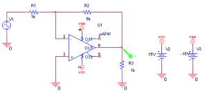
Fig. 3-1 – Circuit used to demonstrate AC Sweep - The ua741 is located in the eval library.
- Instead on wiring the ﺎ15V power supply to the ua741 directly, off page connectors are used. The off page connectors are “virtual wire” which can be used to connect components together.
- To get the off page connector, click on Place/Off-Page Connector,
refer to fig. 3-2. Select the OFFPAGELEFT-R. Place a total
of 4 of them on the schematic.
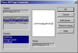
Fig. 3-2 – The Off-Page Connector dialog box. - Change the label on two to Vcc and the other two to Vee.
- Place one Vcc at pin 7 of the ua741 and the other at the 15V power supply.
- Place one Vee at pin 4 of the ua741 and the other at the –15V power supply.
- For the voltage source, select vsin. Vsin is found in the source library.
- For vsin, type in 1V for the Vampland 60 for the Freq.
- Label the output node, pin 6 of the op-amp as out.
- Label the input node, between the voltage source and R1 as in.
- Label the negative node of the op-amp, pin 2, as vn.
- Label the positive node of the op-amp, pin 3, as vp.
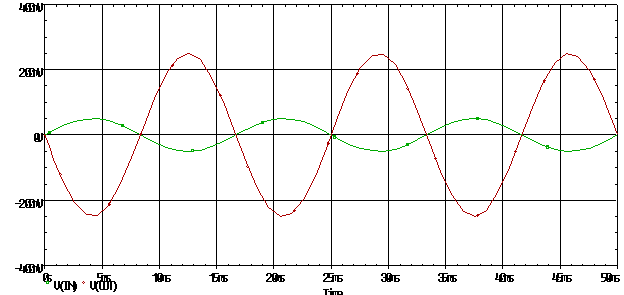
- Create a transient analysis to make sure the op-amp does amplify the signal, refer to fig 3-3 to see the transient analysis result.
|
|
|
Fig. 3-3 – Transient analysis for inverting op-amp configuration |
Sec. 3.2 Setting up the AC Sweep.
To enable an AC Sweep, only a certain voltage source can be sweep, vsin is not one of them. Vsin is can be used only in DC Sweep and transient analysis. Delete the vsin and replace it with vac.
- VAC is located in the SOURCE library.
- Setup a new simulation profile.
- For the simulation, select AC Sweep/Noise in the analysis type.
- Under the AC Sweep type, type in the following:
- 10 for the starting frequency
- 1Meg for the ending frequency
- 101 for the Points/Decade
- Click on logarithm and decade.
- Click OK.
- Run the simulation.
Sec. 3.3 Creating a Bode Plot.
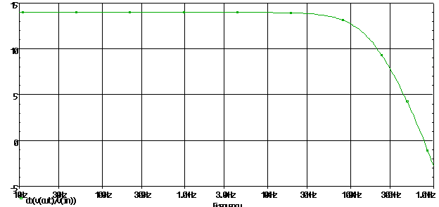
- In the probe window, add a trace that will show the transfer function of the op-amp, which is the Vout/Vin.
- Type in db(v(out)/v(in)). The db specify to plot the output
in decibels.
*Note: db=20log(x). Only type db(v(out)/v(in)) if the nodes are labeld* - The figure should look like fig. 3-4.
|
|
|
Fig. 3-4 – Bode plot of fig. 1. |
Sec. 3.4 Interpreting the results.
Base on the graph, the gain appears to be constant for frequencies up to 10 kHz. But as the frequency increases, the gain starts to roll off, specifically 20db/decade. To find the f–3db, the easiest way is to go to the edge of the plot when the line starts to roll off. Then using the cursor facility, move down until the difference is about 3 db. This is the f–3db for the graph.
Sec. 3.5 The pure SPICE File
Ua741 frequency response
* include the eval library*
.lib eval.lib
* power supply *
VCC 7 0 dc 15V
VEE 4 0 dc -15V
* an ac voltage source of 1V
Vi 1 0 ac 1mV
R1 1 2 100
R2 2 6 100k
* dummy resistor *
R3 3 0 1k
* specify sub circuit of op-amp*
XOA 3 2 7 4 6 ua741
* ac sweep in decade stating at 1 Hz to 10MegHz with 10 points/dec *
.ac dec 10 1Hz 10megHz
.probe
.end
Plotting is the same as for using the PSpice interface.
Sec. 3.6 VTC for inverting op-amp configuration
Besides just using the AC sweep to find the gain, a VTC (voltage transfer curve), can also be used. The voltage transfer curve is a DC analysis of the circuit..
- Use the circuit in fig. 3-1, but replace the VAC with a DC voltage source.
- Change the reference for the DC voltage source to VDC
- Put an initial value of 1V
- Create a new simulation profile.
- Select DC Sweep as the Analysis Type
- Select Voltage Source as the Sweep Variable
- Type in VDCin the name field.
- Select Linear as the Sweep Type.
- Type in –15Vfor the Start Value
- Type in 15V for the End Value
- Type in 0.5V for the Increment
- Click OK
- Run the simulation
- Place a voltage marker at the output pin of the op-amp.
The VTC is shown in fig. 3-5.
|
|
|
Fig. 3-5 - VTC for inverting op-amp |
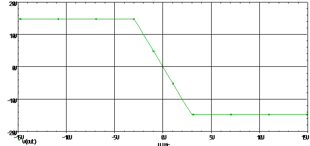
Base on the VTC, it would appear the output is a positive value when the input is negative and negative when the input is positive. Also, the gain can be found by determining the slope of the graph. This is true since the slope is Vout/Vin, or the gain of the circuit.
Sec. 3-7 Transfer function of the inverting op-amp
There is also another way to find the gain of a circuit, and that is to use the .TF option. This option tells PSpice to find the transfer function of the circuit. The transfer function is defined as h(s), which is the impulse response to the circuit.
The .TF is a DC analysis option, consequently, this option should not be used if the frequency response of the circuit is important. The .TF will find the input resistance, output resistance, and the DC gain.
*NOTE – The .TF option will work for any kind of DC source, not just the simple DC voltage source.*
- Use the circuit in fig. 3-1, but place a net alias at the input as
in, and place a net alias at the output as out, refer
to fig. 3-6.
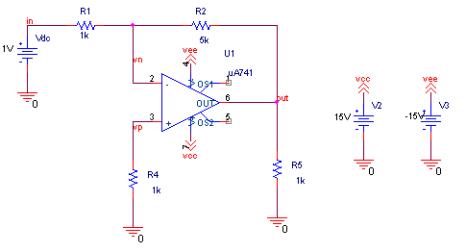
Fig. 3-6 –Circuit to use in .OP simulation - Use a DC voltage source instead of the VAC
- Change the reference to VDC
- Type in an initial value of 1V
- Create a new simulation profile.
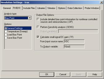
- Select Bias Point as the Analysis Type, refer to fig. 3-7.
- Check the option for Calculate small-signal DC gain
- Type in VDC for the Input Source Name
- Type in V(out) for the Output Variable.
- Click OK
- Run the simulation
|
|
| Fig. 3-7 – Simulation setting dialog box for .TF |
Since the analysis type is a bias point analysis, the graphing functions are disabled. So to view the output, go to the Probe window and click on View/Output File. The following is an excerpt of the output file, to see the complete file, refer to Appendix V.
****     SMALL-SIGNAL CHARACTERISTICS

V(OUT)/V_Vdc = -5.000E+00

INPUT RESISTANCE AT V_Vdc =  1.000E+03

OUTPUT RESISTANCE AT V(OUT) =  4.577E-03
From the listing, the gain is –5V/V, which is the gain for the inverting op-amp. In addition to the gain, PSpice also calculate the input and output resistance of the circuit. In essence, the .TF option is a way of finding the Thevenin equivalent to a circuit.
**** 03/06/00 00:48:27 ********* PSpice 9.0 (Nov 1998) ******** ID# 0 ********

** circuit file for profile: tras

****     CIRCUIT DESCRIPTION

******************************************************************************

** WARNING: DO NOT EDIT OR DELETE THIS FILE

*Libraries:

* Local Libraries :

* From [PSPICE NETLIST] section of pspice.ini file:

.lib "nom.lib"

*Analysis directives:

.TF V([OUT]) V_Vdc

.PROBE

*Netlist File:

.INC "fig1-SCHEMATIC1.net"

*Alias File:

**** INCLUDING fig1-SCHEMATIC1.net ****

* source FIG1

R_R2         VN OUT  5k

R_R1         IN VN  1k

X_U1         VP VN VCC VEE OUT uA741

V_V3         VEE 0 -15V

V_V2         VCC 0 15V

R_R4         0 VP  1k

R_R5         0 OUT  1k

V_Vdc        IN 0 1V

**** RESUMING fig1-schematic1-tras.sim.cir ****

.INC "fig1-SCHEMATIC1.als"

**** INCLUDING fig1-SCHEMATIC1.als ****

.ALIASES

R_R2            R2(1=VN 2=OUT )

R_R1            R1(1=IN 2=VN )

X_U1            U1(+=VP -=VN V+=VCC V-=VEE OUT=OUT )

V_V3            V3(+=VEE -=0 )

V_V2            V2(+=VCC -=0 )

R_R4            R4(1=0 2=VP )

R_R5            R5(1=0 2=OUT )

V_Vdc           Vdc(+=IN -=0 )

_    _(vcc=VCC)

_    _(vee=VEE)

_    _(vn=VN)

_    _(vp=VP)

_    _(out=OUT)

_    _(in=IN)

.ENDALIASES

**** RESUMING fig1-schematic1-tras.sim.cir ****

.END

**** 03/06/00 00:48:27 ********* PSpice 9.0 (Nov 1998) ******** ID# 0 ********

** circuit file for profile: tras

****     Diode MODEL PARAMETERS

******************************************************************************

X_U1.dx         X_U1.dy

IS  800.000000E-18  800.000000E-18

RS    1               1.000000E-03

CJO                   10.000000E-12

**** 03/06/00 00:48:27 ********* PSpice 9.0 (Nov 1998) ******** ID# 0 ********

** circuit file for profile: tras

****     BJT MODEL PARAMETERS

******************************************************************************

X_U1.qx

NPN

IS  800.000000E-18

BF   93.75

NF    1

BR    1

NR    1

CN    2.42

D     .87


**** 03/06/00 00:48:27 ********* PSpice 9.0 (Nov 1998) ******** ID# 0 ********

** circuit file for profile: tras

****     SMALL SIGNAL BIAS SOLUTION       TEMPERATURE =   27.000 DEG C

******************************************************************************

NODE      VOLTAGE   NODE      VOLTAGE    NODE      VOLTAGE     NODE     VOLTAGE

(IN)      1.0000    (VN)      -30.83E-06 (VP)      -79.69E-06  (OUT)    -4.9998

(VCC)     15.0000   (VEE)     -15.0000   (X_U1.6)  557.2E-06   (X_U1.7)  -5.2998

(X_U1.8)  -5.2998   (X_U1.9)  0.0000     (X_U1.10) -.6077

(X_U1.11) 14.9600   (X_U1.12) 14.9600

(X_U1.13) -.5938    (X_U1.14) -.5939

(X_U1.53) 14.0000   (X_U1.54) -14.0000

(X_U1.90) -5.9997   (X_U1.91) 40.0000

(X_U1.92) -40.0000  (X_U1.99) 0.0000


VOLTAGE SOURCE CURRENTS

NAME         CURRENT

V_V3         1.667E-03

V_V2        -1.667E-03

V_Vdc       -1.000E-03

X_U1.vb      5.572E-09

X_U1.vc      1.900E-11

X_U1.ve      9.095E-12

X_U1.vlim   -6.000E-03

X_U1.vlp    -4.600E-11

X_U1.vln    -3.400E-11

TOTAL POWER DISSIPATION   5.10E-02  WATTS

****     SMALL-SIGNAL CHARACTERISTICS

V(OUT)/V_Vdc = -5.000E+00

INPUT RESISTANCE AT V_Vdc =  1.000E+03

OUTPUT RESISTANCE AT V(OUT) =  4.577E-03

JOB CONCLUDED

TOTAL JOB TIME             .26