Objective:
By the end of this lecture, it is hope that the students will have a rudimentary knowledge of using and running PSpice. The student will be able to draw and edit a basic schematic. And lastly, the student will be able to perform a DC nodal analysis.
PSpice GUI
PSpice by definition is a special version of SPICE. In normal SPICE, a circuit is described by text and saved in a CIR file. PSpice contains a GUI interface so the user can easily see the circuit. This helps facilitate the development of large scale projects without the need of figuring how to describe the circuit in words.
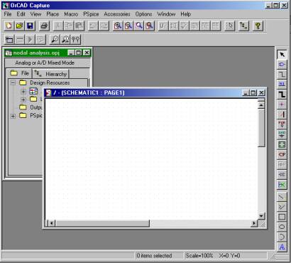
Fig. 1-1 show the main window of Orcad Capture. Every project you work on will start from Orcad Capture.
|
|
|
| Fig. 1-1 Orcad Capture Main window. |
Sec. 1.1 Drawing a Basic Circuit and Nodal Analysis
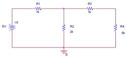
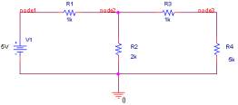
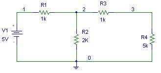
Orcad Capture allows us to draw a circuit visually on the screen, this allows us to easily edit and do analysis on the circuit. Look at fig. 1-2, this is a basic circuit with a independent DC voltage source and a number of resistors. For this lecture, we will be using this circuit. From this basic circuit, you will learn how to simulate and perform a DC nodal analysis. And if time permitting, you will also learn how to write a SPICE file that will describe the circuit.
 |
|
| Fig. 1-2 – Simple circuit. | |
Sec 1.2 How to Create a PSpice project
- From the Start Menu, choose Orcad Capture CIS.
- Click on File/New/Project.
- In the Location area, choose a working directory, refer to fig. 1-3. (It is recommended that you use the hard drive to allow faster simulation.)
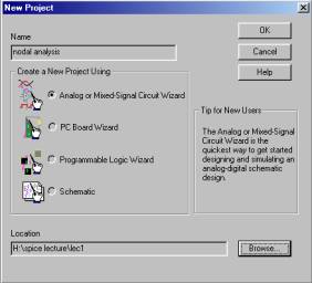 |
| Fig. 1-3 – New project dialog box |
- In the Name area, type in a name for your project, refer to fig. 1-3.
- In the Create a Project Using area, choose Analog or Mixed-Signal Circuit Wizard, refer to fig. 1-3.
- A new window will popup, refer to fig. 1-4. Accept the default by clicking on finish.
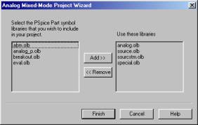 |
| Fig. 1-4 – The library dialog box. |
Sec. 1.3 How to place the voltage source
- In Capture, switch to the schematic page editor. To do this, click on the window that is labeled Schematic Page 1
- Click on Place/Part, or pressing P on the keyboard, to access the Place Part dialog box, refer to fig. 1-5.
|
|
| Fig. 1-5 – Place Part dialog box. |
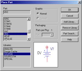
- In the Libraries area, choose SOURCE.
- In the Part area, you can either type in VDC or scroll down until you see VDC
- Click OK.
- Place the part in the schematic by placing the cursor in the schematic area, then click on the left mouse button once.
- Rotate the voltage source by pressing R on the keyboard.
- Press ESC on the keyboard to end placing the part.
Sec. 1.4 How to place the resistors
- Click on Place/Part, or pressing P on the keyboard, to access the Place Part dialog box, refer to fig. 1-5.
- In the Libraries area, choose ANALOG.
- In the Part area, type in R or scroll down until you see R.
- Click OK.
- Place the part in the schematic by placing the cursor in the schematic area, then click on the left mouse button once.
- Place additional resistors by clicking on the left mouse button.
- To rotate the resistors, press R on the keyboard.
- Press ESC on the keyboard to end placing part.
Sec. 1.5 How to place the ground
- Click on Place/Ground to access the Place Ground dialog box, refer to fig. 1-6.
|
|
| Fig. 1-6 – Place Ground dialog box |
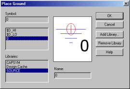
- In the Libraries area, choose SOURCE.
- In the Symbol area, type in 0 or scroll down until you see 0.
- Click OK.
- Place the part in the schematic by placing the cursor in the schematic area, then click on the left mouse button once.
- Press ESC on the keyboard to end placing part.
Sec 1.6 How to connect the parts together
- Click on Part/Wire, or press W on the keyboard, to begin wiring the parts. The pointer should change to a crosshair.
- Click on the connection point, the ends of the parts that is rectangular in shape. Drag the pointer from on element to another element, refer to fig. 1-7.
- Repeat until all the parts are connected together.
|
|
| Fig. 1-7 – How to connect the element |

Sec 1.7 How to change the values of the resistors and the voltage source.
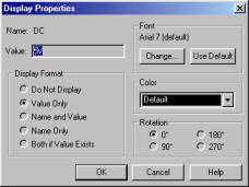
- Double click on the 0V next to the voltage source symbol, refer to fig. 1-8, to access the Display Properties dialog box.
- In the Value area, type in 5V
- Click OK.
- Double click on the 1k next to R1 to access the Display Properties dialog box.
- In the Value area, type in the appropriate value.
- Click OK.
- Repeat for the rest of the elements.
|
|
| Fig. 1-8 – Display Properties dialog box |
Sec. 1.8 How to assign names (labels) to the nets (node)
- Click on Part/Net Alias to access the Place Net Alias dialog box, refer to fig. 1-9.
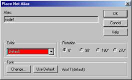 |
| Fig. 1-9 – Place Net Alias dialog box |
- In the Alias area, type in node1
- Click OK.
- Place it on the wire between the voltage source, V1, and R1, refer to fig. 1-10.
- Repeat until your circuit look like fig. 1-10
 |
| Fig. 1-10 – Circuit with net alias |
Sec. 1.9 – How to setup a nodal analysis simulation.
- In Capture, switch to file area by clicking on Analog or A/D Mixed Mode window.
- Click on PSpice/New Simulation Profile to access the New Simulation dialog box, refer to fig. 1-11.
|
|
|
Fig. 1-11 – New Simulation dialog box. |
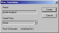
- In the Name area, type in nodal analysis.
- In the Inherit From, choose none.
- Click Create.
- The Simulation Setting dialog box should popup, refer to fig. 1-12.
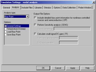 |
| Fig. 1-12 – Simulation Settings dialog box |
- In the Analysis area choose bias point.
- Click OK
Sec. 1.10 – How to simulate the circuit within Capture
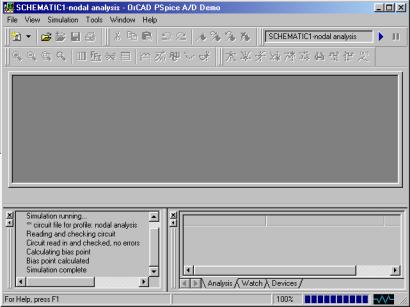
- Click on PSpice/Run.
- The Probe window should open, refer to fig. 1-13.
- In the Probe window click on View/Output.
- Scroll down the window to see all the analysis, refer to Appendix I for the full file.
- Since we are only calculating the bias point, you can’t graph anything.
Sec. 1-11 – How to interpret the result. (See Appendix I)
Let’s say we wanted to know what is the voltage drop and the current flowing through R1. From the schematic, R1 is between node1 and node2. Base on the output file, refer to Appendix I, node1 is 5V and node2 is 3V. The voltage drop then would be:
VR1 = node1 - node2 = 5V - 3V = 2V
IR1 = (node1 - node2)/R1 = (5V - 3V)/1k = 2mA
 |
| Fig. 1-13 – Probe window |
SPICE File Writing
There is a distinct difference between PSpice and SPICE. PSpice is GUI based while SPICE is text based. In this part, you will learn how to translate the circuit shown in fig. 1-3 into a SPICE file.
From the start menu, open PSpice A/D Demo. The probe window should open, refer to fig. 1-13. Click on File/New/Text File.
There is a certain procedure in writing a SPICE file. Although each person will write their file different, the overall procedure is the same way. The first thing to do is to give the circuit a name. Next, describe how the elements are connected together. Include any analysis that is to be performed.
I have found the easiest way to begin is to label the nodes in the circuit. Fig 1-14 show the circuit of fig. 1-3 but with the nodes labeled.
|
|
| Fig. 1-14 – Circuit for SPICE |
Below is the file that should be type and saved. Orcad Probe window is very picky about the file extensions, so it is necessary to type in the CIR extension to the file name when saving.
Simple node analysis example
* Title block *
Vs 1 0 dc 5V
* Voltage source *
R1 1 2 1k
R2 2 0 2k
R3 2 3 1k
R4 3 0 5k
* Resistor network *
.end
This file simple describe the schematic as shown in fig. 1-8. The first line is the title block. This is a name that you give to the circuit. The second line describes the voltage source, called Vs, going from node 0 to node 1. It is a DC voltage source of 5V. Similarly, each resistor is described as being connected between two nodes with a certain value. The last line, .end, is to tell Spice that this the end. A few things to note about the file:
- Any text found after a “*” is considered comments and will not be “compiled” by Spice.
- The 0 node is considered ground or reference node.
- All Spice file must have a title.
- All Spice file must end in .end.
After typing in the Spice file, the file must be saved with a .cir extension (I saved my file as nodal.cir. Once the file is saved, go ahead and simulate the file.
Before you can simulate the file, there is a little thing that must be done. First close the file, then reopen the file by clicking on File/Open Simulation to reopen the file again. The reason you have to do this is because when you type in the file, the file was considered a text file, not a simulation file. So to be able to simulate the circuit, you would have to open the file as a simulation file. I think this is ridiculous way to do this, but it’s the only way that I have got it to work.
To simulate the circuit, click on Simulation/Run. To view the output, click on View/Output, refer to Appendix II for the output file.
Specs. For Common Used Source
PULSE WAVEFORM
|
|
| Pulse waveform used in SPICE |
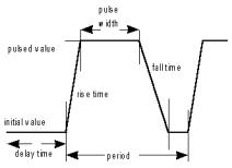
PSpice parameters
TR – Time rise
TF – Time fall
PER – Period of wave
PW – Pulse width
V1 – The minimum voltage/current
V2 – The maximum voltage/current
TD – Time Delay
Spice format
<SoureName> <+node> <-node> PULSE(<v1> <v2> <td> <tr> <tf> <pw> <per>)Format example
Vs 1 0 PULSE(0V 5V 0s 0.05ms 0.05ms 0.5s 1s) – This is for a voltage
pulse waveform
Is 1 0 PULSE(0V 5V 0s 0.05ms 0.05ms 0.5s 1s) – This is for a current
pulse waveform
Example
Creating a pulse wave with a peak voltage at +5V and –5V with a frequency of 60 Hz with no delay.
The first thing to do is to translate the frequency to time. The period is found by using the equation T=1/f. So the period for 60Hz is 16.67ms. The Pulse width need to be half of the cycle so PW would be (1/2)T or 8.34ms. A pulse should ideally have zero time rise and time delay so make TR and TF very small but the same. For this example, 0.0005m is picked. The final SPICE file would be:
Vs 1 0 PULSE (-5V 5V 0s 0.0005m 0.0005m 8.34ms 16.67ms)
Or for a current pulse
Is 1 0 PULSE (-5A 5A 0s 0.0005m 0.0005m 8.34ms 16.67ms)
* Note: In capture, the pulse is split into VPULSE and IPULSE. In SPICE, the user specify either voltage or current source. *
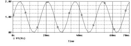
Sinewave
|
|
| Sinewave |
PSpice parameters
DF – Damping CoefficeientsVOFF – DC Offset
VAMPL – Amplitude
FREQ – Frequency
TD – Time Delay
PHASE – Phase of sinewave
SPICE Format
<SourceName> <+node> <-node> SIN(<voff> <vampl> <freq> <td> <df> <phase>)
Format example
Vs 1 0 SIN(0 25mV 120Hz 0 0 0) – This is a voltage sinewave
Is 1 0 SIN(0 25mV 120Hz 0 0 0) – This is a current sinewave
Example
Create a sinewave with a peak voltage of 1V with a frequency of 60Hz with a DC offset of 1V.
Vs 1 0 SIN(1V 1V 60 0 0 0)
Or for a current waveform
Is 1 0 SIN(1A 1A 60 0 0 0 )
|
|
| Sinewave from example |
AC Voltage/Current Source
The Vac voltage source is used most commonly in an AC Sweep mode. To do a bode plot, use a Vac.
PSpice parameters
ACMAG – Magnitude valueACPHASE – Phase value
SPICE format
<SourceName> <+node> <-node> ac ACMAG ACPHASE
Example
Vs 1 0 ac 10 0Or for current source
Is 1 0 ac 10 0
*Note: To create a bode plot in the plot window, it is a good idea to specify the output as decibel.*
Most of the time in hand calculations, the output that is obtained are in volts/volts or amps/amps. This is good for a visualization, but in graphing, this is a bad unit to use. It is a good practice to convert the unit volts/volts into decibel. To convert the unit to decibel, use the following formula:
y = 20log10(x)In PSpice, to specify the output in decibel, then place db in front of the expression.
Example
Specify the voltage gain in decibel. The input variable is in and the output variable is out.
To plot the voltage gain in V/V, then the expression would be v(out)/v(in). So, to plot the gain in decibel, all that is needed is to place the expression db in front of it. The final expression is then db(v(out)/v(in)).
DC Voltage/Current Source
VDC is used to simply provide a DC voltage.PSpice pameters
DC – DC magnitudeSPICE format
<name> <+node> <-node> dc DC
Example
Vs 1 0 dc 5VOr for current source
Is 1 0 dc 5A
*Note – The DC source is used most commonly in biasing of a circuit. I would recommend that the positive voltage source label as Vcc and the negative voltage source label as Vee. This would allow easier trouble shooting. Also, this is the standard name used in most books. *Triangular Waveform
A lot of circuit requires a triangular wave, but unfortunately, SPICE does not come with a predefine triangular waveform. To create a triangular waveform, the simplest way is to modify a pulse wave.
The trick here is to know exactly frequency the waveform is suppose to be. Then I use the following rules to determine the parameters of the pulse wave:
- For a saw tooth waveform
- Figure out the period.
- Set the TR, time rise, to a small amount.
(I use nanosecond for millisecond wave and picosecond for a microsecond wave) - Set the TF, time fall, equal to the period.
- Set the PW, pulse width, to a small amount.
(I use the same procedure as in TR to figure out.
- For a triangular waveform
- Figure out the frequency.
- Set the TR, time rise, and TF, time fall equal to half the period.
- Set the PW, pulse width, to a small amount.
Example
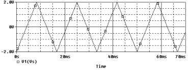
Create a triangular waveform with a peak voltage of ﺎ2V at a frequency of 60Hz.
First thing to do is to determine the period by taking the inverse of frequency. The second thing is to specify a very short pulse with. The tr and tf would be half the frequency.
T = PER = 1/ f= 1/60 = 16.67ms
TR = TF = T/2 = 16.67/2 = 8.33ms
PW = 1ns
Vs 1 0 PULSE(-2 2 0 8.33ms 8.33ms 0.0005ms 16.67ms)
Or for current source
Is 1 0 PULSE(-2 2 0 8.33ms 8.33ms 0.0005ms 16.67ms)
|
|
| Triangular waveform |
**** 03/05/00 22:35:08 ********* PSpice

9.0 (Nov 1998) ******** ID# 0 ********

** circuit file for profile: fig1

****     CIRCUIT DESCRIPTION

******************************************************************************

** WARNING: DO NOT EDIT OR DELETE THIS FILE

*Libraries:

* Local Libraries :

* From [PSPICE NETLIST] section of pspice.ini file:

.lib "nom.lib"

*Analysis directives:

.PROBE

*Netlist File:

.INC "fig1-SCHEMATIC1.net"

*Alias File:

**** INCLUDING fig1-SCHEMATIC1.net ****

* source FIG1

V_V1         NODE1 0 5V

R_R4         NODE3 0  5k

R_R3         NODE3 NODE2  1k

R_R2         0 NODE2  2k

R_R1         NODE1 NODE2  1k

**** RESUMING fig1-SCHEMATIC1-fig1.sim.cir ****

.INC "fig1-SCHEMATIC1.als"

**** INCLUDING fig1-SCHEMATIC1.als ****

.ALIASES

V_V1            V1(+=NODE1 -=0 )

R_R4            R4(1=NODE3 2=0 )

R_R3            R3(1=NODE3 2=NODE2 )

R_R2            R2(1=0 2=NODE2 )

R_R1            R1(1=NODE1 2=NODE2 )

_    _(node1=NODE1)

_    _(node2=NODE2)

_    _(node3=NODE3)

.ENDALIASES

**** RESUMING fig1-SCHEMATIC1-fig1.sim.cir ****

.END

**** 03/05/00 22:35:08 ********* PSpice 9.0 (Nov 1998) ******** ID# 0 ********

** circuit file for profile: fig1

****     SMALL SIGNAL BIAS SOLUTION       TEMPERATURE =   27.000 DEG C

******************************************************************************

 NODE   VOLTAGE     NODE   VOLTAGE     NODE   VOLTAGE

(NODE1) 5.0000    (NODE2)  3.0000     (NODE3) 2.5000

VOLTAGE SOURCE CURRENTS

NAME         CURRENT

V_V1        -2.000E-03

TOTAL POWER DISSIPATION   1.00E-02  WATTS

JOB CONCLUDED

TOTAL JOB TIME             .06
**** 03/05/00 22:38:34 ********* PSpice 9.0 (Nov 1998) ******** ID# 0 ********

Simple node analysis example

****     CIRCUIT DESCRIPTION

******************************************************************************

* Title block *

Vs 1 0 dc 5V

* Voltage source *

R1 1 2 1k

R2 2 0 2k

R3 2 3 1k

R4 3 0 5k

* Resistor network *

.end<

**** 03/05/00 22:38:34 ********* PSpice 9.0 (Nov 1998) ******** ID# 0 ********

Simple node analysis example

****     SMALL SIGNAL BIAS SOLUTION       TEMPERATURE =   27.000 DEG C

******************************************************************************

NODE   VOLTAGE     NODE   VOLTAGE     NODE   VOLTAGE     NODE   VOLTAGE

(1)    5.0000      (2)    3.0000      (3)    2.5000

VOLTAGE SOURCE CURRENTS

NAME         CURRENT

Vs          -2.000E-03

TOTAL POWER DISSIPATION   1.00E-02  WATTS

JOB CONCLUDED

TOTAL JOB TIME             .04
SPICE – Command Line
PSpice is a GUI, graphical user interface, driven program. SPICE is text driven interface. For SPICE, the user must first write a circuit file, then using any SPICE analyzer, the circuit can then be simulate and plot. There are some things to keep in mind when writing a SPICE file, the most important thing is to make sure the SPICE file is supported by the SPICE analyzer. The PSpice that is being used in school support the standard SPICE format, SPICE 3, and also some proprietary tags. So if a SPICE file was specifically written to run in PSpice, and if for some reason the SPICE file was run in a different analyzer, then the user would have to modify the PSpice specific tags to accommodate the targeted SPICE analyzer.
File Format
There is a specific format a SPICE file must follow. Below is how a SPICE file should follow:
Title Statement
Circuit Description
Power supplies / Signal Sources
Element Descriptions
Model Statements
Analysis Request
Output Requests
.END
Title Statement
Like every documents, there should be a title statement. If there is no title statement, the SPICE file will not be simulated. The title statement can be anything.
Circuit Descriptions
This area is where the physical connection of the circuits is described. The valid choices are sources and passive element. The standard sources are as follow:
- Sinewave
- Pulse wave
- DC source
- AC source
- Piecewise linear segment
The standard passive elements are:
- Capacitor
- Diode
- Inductor
- MOSFET
- Resistor
- Transistor
- Transformer
Analysis Request
This tells SPICE what kind of analysis is to be done on the circuit. Below are some analysis options that are available.
|
Command |
Analysis |
Format |
|
.OP |
Operating Point |
. |
|
.DC |
DC Swee[ |
DC <Source name> <Start value><Step value> |
|
.AC |
AC Sweep |
.AC DEC <points/Decade><Start freq.><Stop freq.> |
|
.AC OCT <points/Octave><Start freq.><Stop freq.> |
||
|
.AC LIN<Total points><Start freq.><Stop freq.> |
||
|
.TRAN |
Transient |
.TRAN <Step time><Stop time> [no_print_max_time] [UIC] |
Output Requests
This specify to print only a specific output from the SPICE simulation
.PRINT DC <output variable> - Print data point for DC value
.PRINT AC <output variavle> - Print data point for AC value
.PRINT TRAN <output variable> - Print data points for transient analysis
*NOTE – For .PRINT AC, there are also these following options
- VR, IR – real part
- VI, II – imaginary part
- VM, IM – magnitude
- VP, IP – phase
- VDB, IDB – decibels
There is a .PLOT option, but since the Probe facility provided by PSpice does a better job at plotting waveform, it won’t be go over here.
.END
This just tell SPICE this is the end of the file.
Scale Factors
|
Suffix Letter |
Metric Prefix |
Multiplying Factor |
|
T |
Tera |
10+12 |
|
G |
Giga |
10+9 |
|
Meg |
Mega |
10+6 |
|
K |
Kilo |
10+3 |
|
M |
Milli |
10-3 |
|
U |
Micro |
10-6 |
|
N |
Nano |
10-9 |
|
P |
Pico |
10-12 |
|
F |
Femto |
10-15 |
*Note – if there is no suffix letter to a value, it is assume that it is in standard value, i.e., in volts, ohms, henry, amp, or farad.*