Fun with comparators
A comparator take two voltages and compare them. The output voltage results in a pulse wave with a Vmax = +vsat and Vmin = –vsat. This circuit can be used in creating a gating signal to SCRs or a control signal to a switching mode power supply. (This is a circuit that would be useful in ENGR 455).
For this example, let’s assume the input signal is a sawtooth waveform (vin) with a frequency of 60Hz and and Vmax of 10V. The output signal results in a pulse wave which is 10V if the input voltage is greater than the reference voltage and 0V if the reference voltage is greater than the input voltage. The reference voltage is usually a DC source that the user pick or from a feedback network.
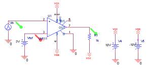
The circuit works by using a LM111, a comparator, with the input voltage coming into the positive pin and the reference voltage coming into the negative pin. The open collector is connected to ground (If the negative voltage need to be less than 0V, then the open collector should be connected to the Vee). The output voltage is pull up to 10V by the means of a pull up resistor. The circuit shown in fig. 5-1 is a possible setup to create the pulse wave.
|
|
| Fig. 5-1 – Comparator circuit with voltage markers. |
Sec. 5.1 Setting up the schematic
- Get the LM111 and place it in the schematic (the LM111 is located in the EVAL library)
- Get the DC voltage source (Use the vdc from the source library)
- Set the voltage corresponding to fig. 1
- Place the ground on the schematic.
- To simplify the placement, use off-page connectors.
- The off page connectors can be place by clicking on Place/Off-Page
Connector
The Off-Page Connectors are virtual wires that connect one parts to another parts. - Place a total of 5 off-page connectors on the schematic. (Select the OffPageLeft-R)
- Label three as vcc
- Label two as vee
- Place the resistor on the schematic
The resistor in the circuit is a pull up resistor. Its primary job is to pull the output level to VCC. - Connect the parts to the LM111
- Pin 4 is the negative power supply
- Pin 8 is the positive power supply
- Pin 2 is the non-inverting input pin (connect this to the input voltage)
- Pin 3 is the inverting input pin (connect this to the reference voltage)
- Pin 1 is the open collector (connect this to the ground)
- Pin 7 is the output pin (connect this to the resistor
- Create the sawtooth waveform
- Set the PER = 16ms
- Set the PW = 16ms
- Set the TD = 0
- Set the TR = 16ms
- Set the TF = 0.001ms
- Set V1 = 0V
- Set V2 = 10V
This setting creates a sawtooth wave of Vpeak of 10V @ 60Hz
Sec. 5.2 Setting the simulation profile
- Create a new simulation profile
- Select a transient response
- Set the Run to Time = 35ms (roughly two cycles)
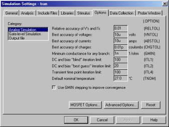
If you run the simulation with just this setting, there will be error messages stating certain elements do not converge. To fix this problem, certain options must be set to ensure convergence does occur.
- Click on PSpice/Edit Simulation Settings
- Click on the Options tab, refer to fig. 5-2
- Set GMIN = 1n (minimum conductance for each branch)
- Set ABSTOL = 10u (Best accuracy for currents)
- Set VNTOL = 10u (Best accuracy for voltages)
- Set RELTOL = 0.10 (Set relative accuracy for voltages and currents)
- Set ITL1 = 100 (DC bias blind limit iteration)
- Set ITL4 = 100 (DC bias best guess iteration)
- Run the simulation.
|
|
| Fig. 5-2 – The option dialog box |
Sec. 5.3 Getting the results
- Select the voltage marker
- Put one voltage marker at Pin 2 of the LM111
- Put one voltage marker at Pin 3 of the LM111
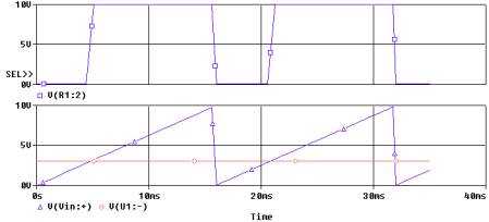
Pin 2 is the input voltage and Pin 3 is the reference voltage. - In the Probe window, do the following
- Click Plot/Add Plot to Window
- Return to the schematic
- Put a voltage marker at Pin 7
This will plot the output voltage wave form - The waveforms should look like fig. 5-3
|
|
|
Fig. 5-3 – The pulse waveform from using a comparator |
Interpreting the results:
Base on the graph, when Vin is less that Vref, the output voltage is 0V. When Vin is greter than Vref, the output voltage is 10V.
Usually we would want the output voltage to have a higher current than the comparator can source, so usually we would place a push-pull pair at the output. Of course this is optional.
Sec. 5.4 Output stage, push pull pair.
Beside the limitation of the current for the comparator, there is also a problem with loading. Sometime the loading of the output could course the output pulse not to reach the desire voltage or an imperfect pulse. One way to compensate this is to put a push pull stage at the output. Once possible configuration for this circuit is shown on fig. 5-4.
|
|
| Fig. 5-4 – Comparator with Push-Pull pair |
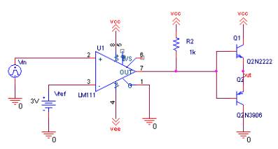
The simulation would output would be similar to fig. 5-3. You would not see any noticeable difference to the circuit until different loads are connected to the output. The QN2222, a NPN transistor, would conduct during the positive cycle of the output wave. The QN3906, a PNP transistor, would conduct during the negative cycle of the output wave.
*NOTE – I have not seen any noticeable difference if the pull up resistor is omitted in this configuration.*