Objective: By the end of this lecture, the students will be able to determine the biasing conditions of a BJT and the input and output impedance.
Sec. 6.1 Family of curves
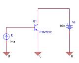
If an amplifier does not have an input signal being applied to it, then the currents and voltages of the BJT are caused by the DC voltage source. This condition is used to determine the operating conditions of a BJT. Consider the circuit shown on fig. 6-1, this circuit can be used in PSpice to determine the operating points of the BJT.
|
|
| Fig. 6-1 – circuit used to find the operating point |
The components used in this simulation are
- DC current source (source library)
- DC voltage source (source library)
- Q2N2222 (eval library)
Build the circuit as shown in fig. 6-1. The values for the voltage source and current source can be any value as long as it’s not zero. For the simulation, we will be using a nested DC sweep. (think of a nested DC sweep as a nested for loop)
After the circuit is build, create a new simulation profile. In the simulation profile, do the following
- In the Analysis type field, select DC Sweep
- In the Sweep variable field, select voltage source and type in Vc, or the name of the voltage source.
- In the Options filed, select Primary Sweep
- In the Sweep type field, select linear
- In the Start value field, type in 0
- In the End value field, type in 10V
- In the Increment field, type in 0.5V
- In the Options field, select Secondary Sweep (Make sure this option is check)
- Select Current Source and type in Ib or the name of the current source
- In the Start value field, type in 0.4mA
- In the End value field, type in 4mA
- In the Increment field, type in 0.9mA
- Click OK
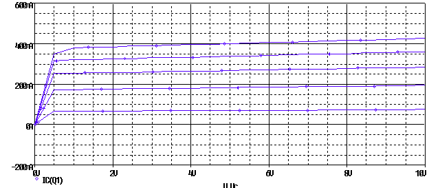
Run the simulation. Now plot the current flowing into the collector either by typing in the expression IC(Q1) or by placing a current marker on the collector of the BJT. The graph you obtain should be similar to fig. 6-2.
|
|
|
Fig. 6-2 – BJT characteristics. |
Sec. 6.2 Example to find Q point
This family of curves shown on fig. 6-2 allows the determination of the operating conditions of the BJTs.
* Note – for the 2N2222, the maximum voltage it can handle is 40V and a maximum current of 600mA
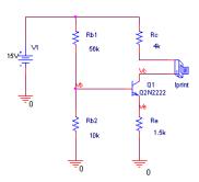
Exercise – finding the Q point of a BJT circuit.
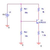
Problem – for the circuit shown in fig. 6-3, determine the operating point of the BJT. Find the value of a) IC, b) IE, c) IB, d)VCE.
|
|
| Fig. 6-3 – Circuit for the exercise. |
Solution
This circuit is a common configuration to bias a transistor. Just to compare the accuracy of PSpice, a hand calculation is done.
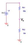
Base voltage
For simplicity, let’s assume that the base current IB is very small compare to the current flowing through RB1 and RB2. Using this assumption, VB can be found using the voltage divider formula, for clarification refer to fig. 6-4.
|
|
| Fig. 6-4 – Circuit used to find VB |
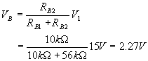
Emitter Voltage
|
|
| Fig. 6-5 – VBE drop of the transistor |
Assuming that the base-emitter junction is a diode drop, VBE can be approximate as 0.7V.
VE = VB - VBE
= 2.27 – 0.7
= 1.57V
Emitter Current
The emitter current is found using Ohm’s law
IE = VE/RE
= 1.57/1.5k
= 1.05 mA
Collector Current
Assuming a very large b, the collector current is approximately the emitter current
IC> IE
Collector Voltage
VC = VCC - RCIC
= 15 – 4k(1.05mA)
= 10.8 V
Collector-Emitter Voltage
VCE = VC - VE
= 10.8 V – 1.57 V =9.23 V
PSPICE Simulation Technique 1
The easiest way to figure out the operating point of the circuit is to perform a bias point calculation. Set up the circuit as shown in fig. 6-3. Create a new simulation profile. For the analysis type, select Bias Point. Run the simulation to get the results. The outcome will be similar to the listing below.
NODE VOLTAGE NODE VOLTAGE NODE VOLTAGE NODE VOLTAGE
(VB) 2.2187 (VC) 10.8270 (VE) 1.5745 (N00041) 15.0000
From the PSpice listing,
IE = 1.5745V/1.5kW = 1.05 mA
VCE = 10.8270V – 1.5745V = 9.2525 V
The values seem to be consistence with our hand calculation.
PSPICE Simulation Technique 2
There is more than one way to determine the operating point of the BJT. This second way is to use a current sensing element to find the current through the branch. The element that will be use is the part name call IPRINT, it can be found in the Special library. The circuit to use the IPRINT is shown in fig. 6-6.
|
|
| Fig. 6-6 – Using IPRINT to fine the current |
- Click on Place/Part.
- Select Special in the libraries field
- If the Special libraries is not present, click on Add library
- Select special.olb
- Click open
- In the Part field, select IPRINT.
- Place the IPRINT part in series with RC.
- The IPRINT acts like an ammeter so it need to be in series with the elements
- Create a new simulation profile.
- Select Bias Point as the simulation type.
- Run the simulation.
The following is an excerpt of the PSpice listing :
NODE VOLTAGE NODE VOLTAGE NODE VOLTAGE NODE VOLTAGE
(VB) 2.2187 (VC) 10.8270 (VE) 1.5745 (N00041) 15.0000
(N00658) 10.8270
VOLTAGE SOURCE CURRENTS
NAME CURRENT
V_V1 -1.272E-03
V_Ic 1.043E-03
This technique stills require the hand calculation for VCE, but the current through RC is found by PSpice.
PSpice Simulation Technique 3
This technique is the simplest by far.
- Create the circuit as shown in fig. 6-3.
- Create a new simulation profile.
- In the Analysis Type select Bias Point.
- In the Output File Options select .OP, refer to fig. 6-7.
- Run the simulation
|
|
| Fig. 6-7 – Simulation profile using .op option. |
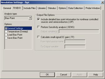
After running the simulation, the output file should contain a listing similar to the one below.
NAME         Q_Q1

MODEL        Q2N2222

IB           6.37E-06

IC           1.04E-03

VBE          6.44E-01

VBC         -8.61E+00

VCE          9.25E+00

BETADC       1.64E+02

GM           4.02E-02

RPI          4.51E+03

RX           1.00E+01

RO           7.92E+04

CBE          5.28E-11

CBC          3.09E-12

CJS          0.00E+00

BETAAC       1.81E+02

CBX/CBX2     0.00E+00

FT/FT2       1.14E+08
This technique does not require any hand calculation at all. PSpice already calculates all the important values for the BJT.
Sec. 7.3 Input and output impedance
BJTs are usually used in amplifier such as the ua741. As with most amplifier, the input and output impedance will vary with frequency. The input and output impedance of the BJT is a concern if it could cause loading to the circuit. For this part, you will learn how to plot the input and output impedance in response to frequency.
- Draw the circuit shown in fig. 6-8
|
|
| Fig. 6-8 – CE amplifier |
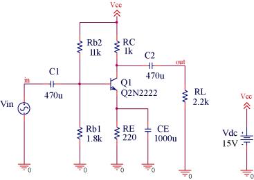
- To confirm that the circuit is indeed an amplifier, create a transient analysis to view the input and output
- For the input voltage source, use Vac
- Create an AC sweep analysis to view the gain.
The above steps is to confirm that the circuit does indeed acts as an amplifier.
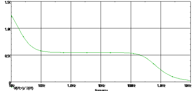
- Simulate the circuit using an AC sweep
- Set the Start frequency to 10 Hz
- Set the End frequency to 10 MegHz
- Set the Points/decade to 101
- Run the simulation
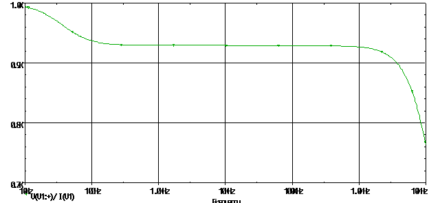
- In the Probe window, add the trace of V(V1:+)/ I(V1), where V1 is the input voltage.
- This would show the input impedance plot vs. frequency, refer to fig. 6-9.
Looking at the plot, the input impedance decreases as the frequency of the input voltage source increases. Also this circuit is a very bad amplifier. The input impedance is too low, it is only about 2 kW. This circuit would cause a significant amount of loading if connected to another circuit. To make this circuit practical, the input impedance would have to increase. This can be done either using an additional stage in front of the circuit, possibly a unity gain MOSFET amplifier, or by removing the biasing resistor Rb1 and Rb2. With the biasing resistor removed, the circuit can be biased using a current source created by using a current mirror.
|
|
|
Fig. 6-9 – Input Impedance plot |
To setup the circuit to find the output impedance, modify the circuit in fig. 6-8 to reflect the change in fig. 6-10.
|
|
| Fig. 6-10 – Output impedance circuit |
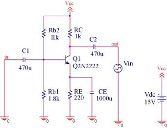
- Change the circuit to fig. 6-10
- Use the same AC sweep setting to find the input impedance
- Simulate the circuit and add the same trace expression for the input impedance
- The plot should look similar to fig. 6-11
The output impedance changes with frequency. So if the input voltage source was to increase, so would the output impedance.
To find the input and output impedance, the IAC source can be used instead of the VAC. With the VAC, the capacitors are needed as to not disturb the biasing condition of the circuit. With the IAC part, it is not necessary to use the capacitors. This is because under DC condition, a current source acts as an open, so the current source would in no may disturb the biasing condition.
|
|
|
Fig.6-11 – Output impedance plot |