| Download lab in PDF format - |
|
ENGR 301 – Electrical Measurements Experiment # 5:Ā MOSFET Characteristics and Applications Objective:ĀĀ To characterize n-channel and p-channel enhancement MOSFETS.Ā To investigate basic MOSFET amplifiers.Ā To compare measured and simulated MOSFET circuits. Components:Ā 2 x CD4007UB MOSFET Arrays, 2 x 0.1 mF capacitors, 1 x 10 kW potentiometer, and miscellaneous resistors: 1 x 100 W,Ā 4 x 10 kW, and 1 x 1 MW (all 1%, ╝ W).Ā Instrumentation:Ā A bench power supply, a signal generator (sine/triangle wave), a digital multimeter, and a dual-trace oscilloscope.Ā References:Ā
Theoretical Background:Ā When an n-channel MOSFET (nMOSFET) is biased in the active region, also called pinchoff or saturation region, and defined by the conditions
its drain current iD is related to the applied gate-source voltage vGS and the operating drain-source voltage vDS as
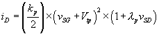
ĀĀĀĀĀĀĀĀĀĀĀĀĀĀĀĀĀĀĀĀĀĀĀĀĀĀĀĀĀĀĀĀĀĀĀĀĀĀĀĀĀĀĀĀĀĀĀĀĀĀĀĀĀĀĀĀĀĀĀĀĀĀĀ ĀĀĀĀĀĀĀĀĀĀĀĀĀ ĀĀĀĀĀĀĀĀĀĀĀĀĀĀĀĀĀ ĀĀĀĀ where kn, a scale factor whose units are A/V2, is called the device transconductance parameter;Ā Vtn is called the threshold voltage; Āand ln, whose dimensions are V-1, is called the channel length modulation parameter (ln is the reciprocal of the Early voltage VA of BJTs, or ln= 1/VAn).Ā For low power MOSFETs, kn is typically in the range of 101 to 102 mA/V2, Vtn is in the range of a few V, and ln is on the order of 10-1 to 10-2 V-1.Ā A given pair of values ID Āand VDS in the iD-vDS plane define a unique point called the operating point Q(ID, VDS) of the MOSFET. The device transconductance parameter kn depends on device geometry as
ĀĀĀĀĀĀĀĀĀĀĀĀĀĀĀĀĀĀĀĀĀĀĀĀĀĀĀĀĀĀĀĀĀĀĀĀĀĀĀĀĀĀĀĀĀĀĀĀĀĀĀĀĀĀĀĀĀĀĀĀĀĀĀĀĀĀĀĀĀĀĀĀĀĀĀĀĀĀĀĀĀĀĀĀĀĀĀĀĀĀĀĀĀĀĀĀĀĀĀĀĀĀĀĀĀĀĀĀĀĀĀ where k’, also in A/V2, is called the process transconductance parameter; and Wn and Ln, both in mm, are the channel width and channel length of the MOSFET. If Vtn > 0, the nMOSFET is said to be of the enhancement type; if Vtn < 0, it is said to be of the depletion type.Ā The threshold voltage Vtn depends on the body bias voltage VSB as
where Vtn0 is the threshold voltage in the absence of any body bias (VSB = 0);Ā gn, in V1/2, is called the body effect coefficient, and is typically 0.5 V1/2; finally, ffn Āis the equilibrium electrostatic potential of the body, typically 0.3 V.Ā Note that for nMOSFETs the body, or substrate, must never be biased more positive than the source, that is, we must always have VSB│ 0. Similar considerations hold for p-channel MOSFETs (pMOSFETs), provided we reverse all current directions and voltage polarities.Ā Thus, while in an nMOSFET iD flows into and iS flows out of the device, in a pMOSFET iD flows out and iS flows into the device.Ā Moreover, the active region conditions of Eq. (1) become, for a pMOSFET,
Similarly, Eq. (2) is rephrased as
where kp= k’(Wp/Lp) is the device transconductance parameter.Ā If Vtp < 0, the pMOSFET is said to be of the enhancement type; if Vtp > 0, it is said to be of the depletion type.Ā Equation (3) holds for all MOSFETs, regardless of the channel type, while Eq. (4) becomes, for a pMOSFET,
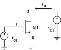
Where now ffp is typically -0.3 V.Ā Note that for pMOSFETs the body, or substrate, must never be biased more negative than the source, that is, we must always have VBS│ 0. MOSFET circuits are readily simulated using PSpice.ĀĀ To this end, we must first create a MOSFET model which, for the case of an n-channel device called our_nMOSFET takes on the form .model our_nMOSFET nmos (kp=kval Vto=Vval lambda=lval gamma=gval) wherekval, Vval, lval, and gval are, respectively, the measured values of k’, Vtn0, ln, and gn. Then, to invoke a transistor MXXX, we use a statement of the type MXXX D G S B our_nMOSFET W=Wval L=Lval where D, G, S,and B are the drain, gate, source, and body terminals, in that specific order, and Wval and Lval are the values of Wn and L n.Ā The following PSpice code uses the circuit of Fig. 1 to display the iD-vDS characteristics of an enhancement nMOSFET called M1 and having Wn= Ln = 10 mm, k’ = 200 mA/V2, Vtn0 = 1.5V, and ln = 0.05 V-1:
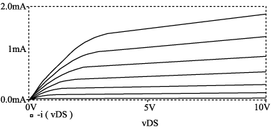
MOSFET Characteristics The characteristics are shown in Fig. 2. The following PSpice code is used to simulate the basic CS amplifier of Fig. 3 using the same MOSFET model of above: CS Amplifier After running PSpice, we obtain an output file with the following information: BIAS SOLUTION:ĀĀĀĀĀĀ NODEĀĀĀ VOLTAGEĀĀĀ NODEĀĀĀ VOLTAGEĀĀĀ NODEĀĀĀ VOLTAGEĀ NODEĀĀĀ VOLTAGEĀĀĀ NODEĀĀĀ VOLTAGEĀĀĀĀĀĀ AC ANALYSIS: ĀFREQĀĀĀ VM(1)ĀĀĀ VP(1)ĀĀĀ VM(5)ĀĀĀ VP(5)ĀĀĀĀ
We readily find the gain of this amplifier to be vo/vs= VM(5)/VM(1) =-0.3991/0.1 = -3.991 V/V, where the negative sign is implied by the fact that VP(5) = -180o.ĀĀ You may find it instructive to confirm the above data (both bias and ac) via hand calculations!
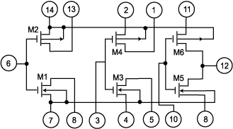
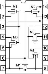
The CD4007UB MOSFET Array: We shall perform our measurements and experiments using the CD4007UB MOSFET Array.Ā This array consists of three nMOSFETs and three pMOSFETs, all of the enhancement type, with the interconnections shown in Fig. 4.Ā Note that the body of the nMOSFETs (pin 7), which is p-type, must always be connected to the most negative voltage (MNV) in the circuit; likewise, the body of the pMOSFETs (pin 14), which is n-type, must always be connected to the most positive voltage (MPV) in the circuit.Ā Failure to respect these constraints may invalidate all measurements taken.Ā
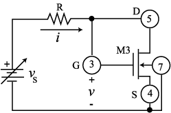
Pinchoff-Region Characteristics: We shall use the circuits of Figs. 5 and 6 to find Vt and k, the circuits of Figs. 7 and 8 to find l, and the circuits of Figs.9 and 10 to find g.Ā In the circuits of Figs. 5 and 6 vS is a variable DC source which is used along with R to establish prescribed values of i.Ā To perform your i and v measurements, first configure your digital multimeter (DMM) as an ammeter in series between the resistance R and the drain D to set i, then as a voltmeter in parallel with the MOSFET to measure v.Ā In case your ammeter has been put it out of service by abuse, you can still use your DMM to perform current measurements as follows:Ā Before inserting R in the circuit, measure it with the ohmeter; then insert R, and while monitoring with the voltmeter the voltage vR across R, adjust vS for the desired value of i (for instance, to obtain i = 100 mA with R = 98 kW, adjust vS until vR = Rx i = 98 x 0.100 = 9.8 V).
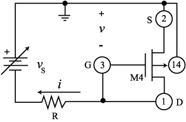
Mark one of your CD4007UB ICs, and as you interconnect parts of it in the circuits below, use short leads and bypass the power supplies with 0.1-mF capacitors, as recommended in Appendix A2.Ā M1:Ā For the nMOSFET of Fig. 5, measure v for the following values of i (shown within parentheses are the correspondingĀ recommended values of R):Ā i = 0.1 mA (100 kW),Ā i = 0.4 mA (20 kW; use 2 x 10-kW resistors in series), and i = 2 mA (5.0 kW; use 2 x 10-kW resistors in parallel).Ā Then, repeat for the pMOSFET of Fig. 6.Ā As usual, all your data should be expressed in the form X▒DX.
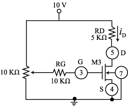
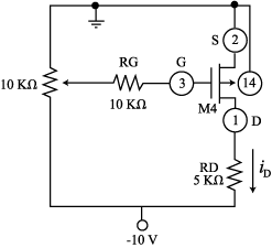
M2:Ā For the nMOSFET of Fig. 7 adjust the potentiometer until VDS = 5 V (for RD use 2 x 10-kW resistors in parallel).Ā Also, record the value of VGS, which will be needed in Step M6.Ā Next, turn off power, configure your DMM as a DC ammeter, break the circuit at node D, insert the ammeter in series, reapply power and measure ID both with RD in place as shown, and with RD shorted out with a wire.Ā The difference DID between the two readings will be small, so make sure to use as many digits as your ammeter will allow.Ā Note that shorting out RD is designed to cause a change DVDS = 5 V. As usual, all your data should be expressed in the form X▒DX.
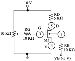
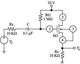
M3:Ā Repeat Step M2 for the pMOSFET of Fig. 8, after having adjusted the potentiometer for VSD = 5 V.ĀĀ Record also the value of VSG, which will be needed in Step M7. C4:Ā Using the nMOSFET data of Step M2, find ron = DVDS /DIDĀ and, hence, ln = 1/VAn = 1/(ronIDĀ - VDS).Ā Likewise, using the pMOSFET data of Step M3, find rop = DVSD /DIDĀ and, hence, lp = 1/VAp = 1/(ropIDĀ - VSD).Ā ĀĀ C5:Ā Let us now introduce the quantities x = vĀĀĀĀĀĀĀĀĀĀ Using the nMOSFET set of i and v data of Step M1, along with the value of ln found in Step C4, calculate the corresponding values of y, plot them on x-y graph paper, and draw the best fit straight line; in view of Eq. 2, the intercept of this line with the x-axis yields Vtn0, and its slope yields (kn/2)1/2, which allows us in turn to find kn.Ā Then repeat the procedure for the pMOSFET, keeping in mind that in this case the intercept of the best fit straight line with the x-axis yields -Vtp0, and its slope yelds (kp/2)1/2, which, in turn, we use to find kp.Ā MC6:Ā Turn power off in the circuit of Fig. 7, lift the p-body (pin 7) off ground, and return it to a –5-V supply via a protective 10-kW series resistor as shown in Fig. 9.Ā Reapply power, adjust the potentiometer until you get again VDS = 5 V, and record the new value of VGS.Ā Then, apply Eq. (4) to find
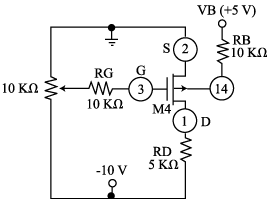
where DVGS is the difference between the current value of VGS and that found in Step M2, and ffn = 0.3 V.Ā MC7:Ā Turn power off in the circuit of Fig. 9, lift the n-body (pin 14) off ground, and return it to a +5-V supply via a protective 10-kW series resistor as shown in Fig. 10.Ā Reapply power, adjust the potentiometer until you get again VSD = 5 V, and record the new value of VSG.Ā Then, apply Eq. (7) to find
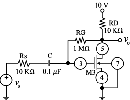
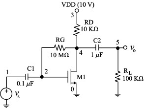
where DVSG is the the difference between the current value of VSG and that recording Step M3, and ffn =Ā -0.3 V. Summarize your numerical findings for kn, Vtn0, ln, gn, and kp, Vtp0, lp, gp, and express all data in the formĀĀ X▒DX. S8:Ā UsePSpice to display the iD-vDS characteristics of your nMOSFET, as well as the iD-vSD characteristics of your pMOSFET.Ā Do it both for the case of 0-V and 5-V body bias.Ā Comment on your findings. Common-Source Amplifier: With power off, assemble the circuit of Fig. 11, keeping the leads short and bypassing the power supply with a 0.1 mF capacitor. C9:Ā Predict the DC voltage VD at the drain terminal in Fig. 11, as well as the small signal gain Av = vo/vs.Ā
M10:Ā While monitoring vs with Ch.1 of the oscilloscope (DC mode, Trigger on Ch. 1), adjust the signal generator so that vs in Fig. 11 is a 10-kHz sinewave with 0-V DC and 0.5-V peak amplitude.Ā Next, use CH. 2 (DC mode, Chop Mode), to measure the DC voltage at the drain pin; finally, switch Ch. 2 to the AC mode and measure the peak amplitude of vo; hence, find the gain Av = vo/vs of your amplifier.Ā S11:Ā Simulate the circuit of Fig. 11 using PSpice.Ā For a realistic simulation, you need to create a PSpice model for your specific nMOSFET sample, using the above measured values of kn, Vtn0, ln, and gn. C12:Ā Compare the predicted values of Step C9 with the measured values of Step M10 and the simulated values of Step S11; account for any possible discrepancies.Ā M13:Ā Returning to the circuit of Fig.11, switch Ch. 2 back to the DC mode (make sure you know where your 0-V baseline is on the screen!), change the input generator’s waveform to triangular, andrise its amplitude until vo distorts both at the top and at the bottom.Ā Justify the two types of distortion in terms of transistor operation.Ā
Common-Drain Amplifier: With power off, assemble the circuit of Fig. 12, keeping leads short and using a 0.1-mF power supply bypass capacitor, as usual.Ā Then, adjust the input source so that vs is a 10-kHz sinewave with 0-V DC and 2-V of peak-to-peak amplitude.Ā CMS14:Ā In Fig. 12 predict the DC voltage VS , as well the small signal gain Av = vo/vi.Ā Next, measure VS and Av.Ā Next, find VS and Av via PSpice.Ā Finally, compare the three sets of values, and account for possible discrepancies. CMOS Amplifier: One of the most popular MOSFET amplifier configurations is the complementary MOS (CMOS) cell of Fig. 13, consisting of an nMOSFET and a pMOSFET with the gates tied together to form the input node, and the drains tied together to form the output node.Ā As you assemble this circuit, keep leads short and use a 0.1-mF power supply bypass capacitor, as usual.Ā Since this stage exhibits a fairly high gain, its input vi must be suitably small, so we interpose a voltage divider R1 and R2 between the input source and the amplifier to suitably scale down the source.Ā With the resistances shown we have vi @ vs/100.Ā C15:Ā For the circuit of Fig. 13 predict the DC output voltage VO as well as the small signal gain Av = vo/vi. M16:Ā While monitoring vs with Ch.1 of the oscilloscope (DC mode, Trigger from Ch. 1), adjust the input signal generator so that vs in Fig. 13 is a 10-kHz sinewave with 0-V DC and 1-V peak amplitude (this makes vi a 10-mV peak amplitude sinewave).Ā Next, use CH. 2 (DC mode, Chop Mode), to measure VO.Ā Now, switch Ch. 2 to the AC mode and measure the peak amplitude of vo; finally,Ā find the gain Av = vo/viof your amplifier.Ā
SC17:Ā Simulate the circuit of Fig. 13 using PSpice; then, compare predicted, measured, and simulated values, and account for any possible discrepancies.
|
||||||||||||||||||||||||||||||||||||||||||||||

 (a)
(a)