| Download lab in PDF format - |
|
ENGR 301 – Electrical Measurements Experiment # 3:Ā Diode Characteristics and Applications Objective:ĀĀ To characterize a rectifier diode and a zener diode.Ā To investigate basic power supplies concepts such as rectification, filtering, and regulation.Ā To investigate basic op amp rectifiers.Ā To compare measured and simulated diode circuits.Ā Components:Ā 1 x 6.3 V CT transformer, 4 x 1N4001 power rectifier diodes, 4 x 1N4148 low power rectifier diodes, 1 x 1N4733 5.1 V, 1 W zener diode, 2 x 741C op amps, 2 x 0.1 mF capacitors, 1 x 100 mF capacitor, and miscellaneous resistors:Ā 1 x 100 W, 2 x 1 kW, 1 x 10 kW, and 6 x 100 kW (all 1%, ╝ W).Ā Instrumentation:Ā A dual ▒15-V regulated power supply, a signal generator (sinewave), a digital multimeter, and a dual-trace oscilloscope.Ā References:Ā
Theoretical Background:Ā A pn junction diode exhibits the well known i-v characteristic
where IS , a current scale factor, is called the saturation current; VT, a voltage scale factor, is called the thermal voltage;Ā n, an empirical constant called the emission coefficient, is in the range of 1 for integrated circuit diodes to 2 for discrete diodes. Engineers use the following two rules of thumb to characterize the behavior of a forward biased diode with n = 1 at room temperature: Ā(a) To effect an octave change in i, we must change v by 18 mV; (b) To effect a decade change in i, we must change v by 60 mV. The parameter IS is a strong function of temperature; moreover, it depends on diode area.Ā As a rule of thumb, IS doubles for every 5oC rise in temperature.Ā For low power IC diodes, IS Āis typically in the range of fAs (1 fA = 10-15 A), though there are diodes with IS in the range of pAs or even nAs.Ā The parameter VT is linearly proportional to absolute temperature, and its room temperature value is VT @ 26 mV.Ā The thermal behavior of a junction diode is also expressed by the following popular rule of thumb:Ā For a junction diode operating at constant current i, the diode voltage drop v decreases (increases) by 2mV for every 1oC rise (drop) in temperature.Ā When a diode is forward biased at nontrivially low currents, we
have exp (v/nVT) >> 1, so Eq. (1) can be
approximated as
This equation indicates that if we perform a set of i-v measurements on a pn diode and then plot them on semilogarithmic paper, with v on the linear axis and i on the logarithmic axis, the resulting curve is a straight line such that for every decade change in current, voltage changes by 2.303nVT .Ā We can exploit this to find the values of IS and nVT experimentally.ĀĀ When a diode is reverse biased, Eq. (1) no longer holds.Ā Rather, the diode exhibits two regions of operation:Ā (a) At moderately low reverse voltages, a diode conducts a current IR called the reverse current.Ā Typically, IR is orders of magnitude larger than IS, and it is likewise a strong function of temperature.Ā As a rule of thumb, IR doubles for every 10oC rise in temperature. (b) As the reverse bias voltage is increased, a point is reached at which the diode becomes strongly conductive, and is said to be operating in the breakdown region.Ā In this case it is notationally convenient to reverse the reference direction of current and the reference polarity of voltage by letting iZ = -i and vZ = -v.Ā The resulting vZ-iZ characteristic is approximately linear, or
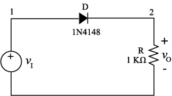
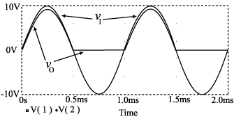
where VZ0 is the extrapolated value of vZ in the limit iZ« 0, and rz is the dynamic resistance of the diode in the breakdown region.Ā Its reciprocal 1/rz Āis the slope of the iZ -vZĀ characteristic.Ā The smaller rz, the steeper the iZ -vZ curve, and the closer the diode behavior to an ideal voltage source.Ā This feature is exploited on purpose in voltage regulation applications.Ā ĀĀĀĀĀĀĀĀĀĀĀĀĀĀĀ Diode circuits are readily simulated using PSpice.Ā The file Eval.lib that comes with the student version of PSpice contains models for popular junction diodes, including the 1N4148 rectifier diode and the 1N750 4.7-V zener diode.Ā For instance, to invoke a 1N4148 diode from the built in library, we use a command of the type DXXX A C D1N4148 where DXXX is the name of the specific diode (such as D1), and A and C are the anode and cathode nodes, in that specific order.Ā Shown below is the PSpice code for the simple diode circuit of Fig. 1. Half-Wave Rectifier The response is shown in Fig. 2.
Experimental Setup: Diodes usually come with a band identifying the cathode terminal (the other terminal is, of course, the anode).Ā If in doubt, you can determine experimentally which terminal is which by measuring the diode with an ohmmeter (the diode must be out of the circuit, and the ammeter’s scale should be set in the kW range).Ā Then, if the display blinks (indicating over range resistance), the cathode is the one connected to the red cable of the ohmmeter; if the display shows some finite resistance, then the cathode is the one connected to the black cable.Ā To make sure, try out both connections and verify that they give consistent results.Ā Henceforth, steps shall be identified by letters as follows: C for calculations, M for measurements, and S for SPICE simulation.Ā Moreover, each measured value should be expressed in the form X▒DX ( e.g. v = 650.5mV ▒ 0.1 mV), where DX represents the estimated uncertainty of your measurement, something you have to figure out based on your learning in ENGR 300.
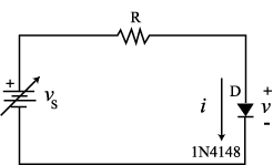
Forward-Region Characteristic: This characteristic shall be obtained by Here vS is a variable DC source which, together with R, is used to establish prescribed values of i.Ā To perform your i and v measurements, first configure your digital multimeter (DMM) as an ammeter in series between the resistance and the diode to set i, then as a voltmeter in parallel with the diode to measure v.Ā In case your ammeter has been put it out of service by abuse, you can still use your DMM to perform current measurements as follows: Before inserting R in the circuit, measure it with the ohmmeter; then insert R, and while monitoring with measuring v for different values of i using the circuitĀ of Fig. 3.voltmeter the voltage vR across the terminals of R, adjust vS for the desired value of i (for instance, to obtain i = 100 mA with R = 98 kW, adjust vS until vR = Rx i = 98 x 0.100 = 9.8 V).ĀĀ M1:Ā In the circuit of Fig. 3 measure v for the following values of i (shown within parentheses are the correspondingĀ recommended values of R):Ā i = 10 mA (1 MW),Ā i = 100 mA (100 kW), i = 1 mA (10 kW), and i = 10 mA (1 kW).Ā As you measure v, use as many digits as your DVM will allow (why?).Ā Hence, plot your data on semilogarithmic paper (v on the linear scale, i on the log scale), with each datum shown as a rectangle with dimensions reflecting the uncertainties of the corresponding measurements, as learned in ENGR 300.Ā C2:Ā Draw a best fit straight line (if you can, do this by computer, using your ENGR 308 learning).Ā Measure its slope, and hence find the value of nVT .Ā Assuming VT = 26 mV, what is the experimental value of n?Ā Finally, find the experimental value of IS.Ā Are your findings typical?Ā Comment.Ā S3:Ā Create a PSpice diode modelwiththe above values of n and IS.Ā Hence, using PSpice as a curve tracer, plot the diode i-v curve both on linear and semilog scales.Ā How does the semilog curve compare with the experimental one you derived?Ā To create a diode model for a specific sample, such as our_diode, we use the statement .model our_diode D (Is=Ival n=nval) where Ival and nval are the measured values of IS and n.Ā Then, to invoke a specific diode of that class, say D1, we use the statement:Ā D1 A C our_diode
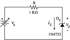
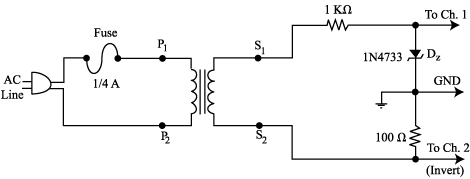
Breakdown-Region Characteristic: This characteristic shall be obtained by measuring vZ for different values of iZ using the circuit of Fig. 4.ĀĀ The suggestions given above in connection with the measurements of Fig. 3 still hold.Ā M4:Ā In the circuit of Fig. 4 measure vZĀ for two different valuesof iZ, say iZ1 = 5 mA and iZ2 Ā= 10 mA.Ā Denoting the corresponding voltages as vZ1 and vZ2, calculate the dynamic resistance of the diode as rZ = (vZ2 - vZ1)/(iZ2 - iZ1).Ā Hence, use Eq. (3) to find the extrapolated value VZ0. M5:Ā Assemble the circuit of Fig. 5 to observe the complete i-v characteristic of the zener diode (for safety, be sure to connect the ╝-A fuse in series with the primary, as shown).ĀĀ Here, the oscilloscope is used in the x-y Mode (see ENGR 206), with the anode voltage v as the x axis (Ch1. 1, 1 V/div, DC), and the cathode current i, sensed across the 100-W resistor, as the y axis (Ch. 2, Inverted, 0.2 V/div, DC).Ā Before connecting the oscilloscope to your circuit, adjust the offsets of the two channels so that the origin of the x-y display (dot) is at the center of the screen.Ā Also, keep the beam intensity suitably low to avoid burning out the phosphor on the CRT.ĀĀĀ
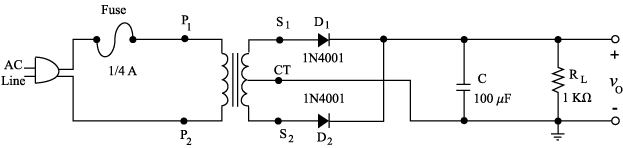
C6:Ā Once you have displayed the i-v characteristic, develop large-signal diode models (with actual element values) for the three regions of operation, namely, forward, cutoff, and breakdown.Ā Simple DC Power Supply: For thefollowing investigations, refer to Fig. 6.Ā Before assembling the circuit downstream of the secondary, observe the waveforms at nodes S1 and S2 with the oscilloscope (center tap to ground of the oscilloscope, vS1 to Ch. 1, vS2 to Ch. 2, Trigger from Ch.1, Chop Mode), and verify that they are out of phase with each other.Ā What are their amplitudes Vm1 and Vm2?Ā MC7:Ā Assemble the circuit of Fig. 6, but without interconnecting D2 and C yet.Ā Observe vS1 and vOwith Ch.1 and Ch. 2 of the oscilloscope, and use the information provided by Ch. 2 to predict the average (or DC) value VO of vO (show your calculations!).Ā Then, measure VOwith the DC voltmeter, compare with the predicted value, and account for any discrepancies.Ā What is the maximum reverse voltage (PIV) that D1must withstand?
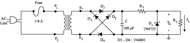
MC8:Ā Now connect C, but with D2 Āstill disconnected.Ā Predict the output ripple as well as the new DC value of vO(show your calculations!).Ā Observe the ripple with Ch. 2 (switch it to the AC mode for this observation,), measure VO with the DC voltmeter, compare with your predictions, and comment.Ā What is now the PIV for D1? MC9:Ā Repeat first Step MC7, and then Step MC8, but also with D2 in place.Ā Hence, summarize the advantages of using also D2. Zener Diode Regulator: For thefollowing investigations, refer to Fig. 7, which is intended to be a DC power supply of aboutĀ 5 V with a maximum current rating of about 10 mA, or 0 <Ā IL < 10 mA. C10:Ā Based on the observations and measurements of the previous steps, calculate a suitable value of Rs in the circuit of Fig. 7 for a maximum load current of 10 mA.Ā Then, obtain from the stockroom a standard resistor closest to the calculated value, and predict both the load regulation and the output ripple of your circuit.ĀĀ M11:Ā Assemble the circuit of Fig. 7, and observe the voltage across C with Ch.1 of the oscilloscope, and the voltage across Dz with Ch.2 of the oscilloscope (you may alternate between the DC and AC Modes, as needed, for optimal observations).Ā Measure the output ripple with the oscilloscope and VO with the DC voltmeter at the following two extremes:Ā RL = ź (no load) and RL = 500 W (maximum load; use 2 x 1 kW Resistors in parallel).Ā What is the measured load regulation of your circuit?Ā The measured output ripple?Ā Compare with the predictions of Step C10, comment.Ā Precision Rectifiers:
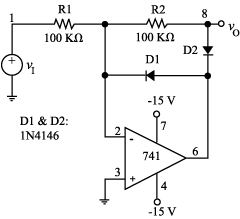
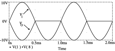
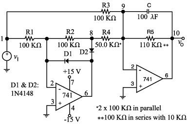
As shown in Fig. 2, the diode voltage drop results in a error which may be undesirable, especially in precision rectifier applications.Ā This error can be nullified by placing the diode (or diodes) within the feedback loop of an op- amp.Ā Figure 8 shows a popular example of a precision half wave rectifier using this concept.Ā The circuit is readily simulated via PSpice using the following code:Ā Precision Half-Wave Rectifier As shown in Fig. 9, the circuit gives (a) vOĀ = -vIĀ for vI Ā> 0, and vO = 0 for vI < 0, and it does so without appreciable errors due to the nonzero diode drops.ĀĀ M12:Ā Assemble the circuit of Fig. 8 (see Appendix 2 for useful tips), and confirm its behavior by monitoring vIĀ and vOĀ with Ch.1 and Ch. 2 of the oscilloscope (both Channels set on DC, Trigger from Ch. 1, Chop Mode).Ā Next, use Ch. 2 to observe the waveform at the output of the op amp (pin 6), and justify it by analyzing the behavior of the circuit first for the case vIĀ > 0, then for the case vI < 0.Ā Finally, gradually rise the input frequency until you begin to observe appreciable distortion at the output.Ā Hence, justify this distortion in terms of well known op amp limitations.ĀĀĀ C13:Ā By summing a signal with its half wave rectified version in a 1:2 ratio, we obtain the precision full wave rectifier of Fig. 10.Ā Prove that its output is vOĀ = (R5/R3) x |vI|, this being the reason why the circuit is also called a precision absolute value circuit.Ā Hint: Consider first the case vIĀ > 0, then the case vIĀ < 0.
S14:Ā Use PSpice to display the input and output waveforms of the circuit of Fig. 10 for the case in which C is not connected yet.Ā M15:Ā Assemble the circuit of Fig. 10 to confirm the waveforms of Step S14.Ā Next, connect C as shown. This turns the summing op amp into a low pass filter to yield VOĀ = (R5/R3) x Avg(|vI |), where Avg(|vI |) denotes the average of |vI |.Ā Recall that if vI is a sinewave of amplitude Vm, then Avg(|vI |) = (2/p)Vm = 0.637Vm.Ā Amplifying this average by R5/R3 = 110/100 = 1.1 gives VO = 0.707Vm, which coincides with the rms value of ĀvIĀ when vI is an ac signal.Ā Verify that this is the case by letting vI be a sinewave with zero DC offset, but variable amplitude and frequency;Ā then, while monitoring ĀvIĀ with the AC voltmeter and VO with the DC voltmeter, compare the two readings for several amplitudes and frequencies of ĀvI, and account for possible discrepancies.Ā The circuit of Fig. 10 forms the basis of a class of AC voltmeters known as averaging type ac voltmeters.Ā Can you justify?
|