| Download lab in PDF format - |
|
ENGR 301 – Electrical Measurements Experiment # 1:Ā Time and Frequency Responses of Series RLC Circuits Objective:ĀĀ ToĀ investigate the step and frequency responses of series RLC circuits.Ā To compare experimental results with theory and PSpice simulations, and account for possible discrepancies.Ā To familiarize the student with Bode plots.Ā Components:Ā 1 x 3.9-mHĀ inductor, 1 xĀ 10-nF capacitor, 1 x 500-W potentiometer, and miscellaneous resistors: 1 x 10 W, 1 x 100 W, 1 x 1.0 kW, and 1 x 2.0 kW (all 5%, ╝ W). Instrumentation:Ā An RLC meter, a signal generator (squarewave, pulse and sinewave), and a dual-trace oscilloscope.Ā References:Ā
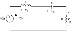
Theoretical Background:Ā RLC circuits are classical examples of second order systems.Ā Together with their mass-spring-dashpot mechanical analog, they are widely used to illustrate fundamental systems-theory concepts and techniques, such as Laplace transform techniques and resonance. The current response of the series RLC circuit of Figure 1
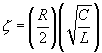
is found via Laplace transform techniques asĀ I(s) = Y(s)V(s), where I(s) and V(s)are the Laplace transforms of i(t) and v(t), s is the complex frequency,Ā and Y(s) is the complex admittance, that is, the reciprocal of the complex impedance Z(s),.
This function is usually expressed in the standardized form
where w0 is the undamped natural frequency and zis the damping ratio.Ā The values of these parameters are set by those of the components making up the circuit ĀĀĀ ĀĀĀĀĀĀĀĀĀĀĀ The values of s for which the denominator of Y(s) becomes zero are called the poles of Y(s), and therefore, the zeros of Z(s).Ā They are easily found to be
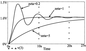
For z > 1, the poles are real and distinct, and the system is said to be overdamped;Ā for z = 1, the poles are real and coincident, and the system is said to be critically damped.; for 0 < z < 1, the poles are complex conjugate, and the system is said to be underdamped.ĀĀ In each of the above cases the poles lie in the left half of the complex plane s.Ā For z = 0, the poles lie right on the imaginary axis, and the system is said to be undamped.Ā It is apparent that varying R while keeping L and C constant R moves the poles around in the complex plane. Systems theory indicates that the response i(t) to a given excitation v(t) can be found as i(t) = ĀL-1{I(s)} = L-1{Y(s)V(s)}, where L -1 indicates inverse Laplace transformation.Ā The responses of greatest practical interest in engineering are the impulse, the step, and the ac responses.Ā The current response i(t) is readily visualized with the oscilloscope by observing the voltage vR(t) across the resistance R; then, i(t) = vR(t) /R.Ā Of great interest are also the capacitance and inductance responses vC(t) and vL(t). All responses can readily be visualized by means of PSpice.Ā The following PSpice code is used to visualize the step and ac responses for the case w0Ā = 1 rad/s and ĀzĀ = 1.Ā The code is readily adapted to other values of w0 and z. Series RLC Circuit Figure 2 shows the step response vC(t) across the capacitor for three different values of z.ĀĀ
It can be proved that for z < 1this response is a damped sinusoid with frequency
We also observe the presence of overshoot, defined as OS (%) = 100[vC(peak) Ā- vC(t «ź]/vC(t «ź).Ā The overshoot is related to zĀ as
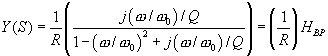
The smaller the value of z, the higher the overshoot and the longer it takes for the oscillation to die out.Ā In the limit z«0 we have a sustained oscillation with frequency w0.Ā If zĀis gradually increased from zero, the oscillation will die out more and more rapidly until the point is reached where there will be no more oscillation.Ā This point corresponds to critical damping, or zĀ= 1.Ā For zĀ >1, not only is there no oscillation, but the system takes even a longer time to reach its steady state. ĀĀ ĀĀĀĀĀĀĀĀĀĀĀĀ Systems theory indicates that the frequency response of a circuit is readily found by letting s «Ā jwĀ in its transfer function.ĀĀ In this case it is also more common to work with the parameter Q = 1/2z , after which our expression above becomes
where HBP is called the standard second order band pass function.ĀĀ To investigate the frequency response of our circuit, we apply an ac voltage v(t) of the type Vim cos wt, and we observe the response vR(t) = Ri(t) across the resistor, which is is an ac voltage of the type Vom cos (wt + f),Ā where Vim and Vom are peak amplitudes (in V), w is angular frequency (in rad/s), and f is phase angle (in degrees).ĀĀ The parameters of the response are related to those of the applied voltage asĀĀ
where |HBP|Ā and ąHBP are, respectively, the magnitude and phase of HBP.Ā Figure 3 shows the logarithmic plots of magnitude and phase, also called Bode plots, for three different values of Q.Ā
ĀĀĀ ĀĀĀĀĀĀĀĀĀĀĀ Each magnitude curve peaks at 0 dB for w=w0, this being the reason why w0 is also called the resonance frequency.Ā Moreover, each curve drops to –3 dB at two frequencies wLand wH such that
It is readily seen that these frequencies satisfy the condition wLxwHĀĀ = w02, and that phase is ▒450 at these frequencies.Ā Moreover, the half power bandwidth, defined as BW = wH – wL, is such that
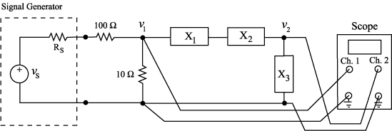
It is apparent that the narrower BW for a given w0, the higher its Q.Ā Consequently, Q provides a measure of the degree of selectivity of a filter circuit such as ours. Experimental Setup: To lower the output resistance of the function generator (typically on the order of 50 W) to a more predictable value, we interpose a voltage divider as shown in Fig. 4.Ā Note that because of the internal ground connection of the oscilloscope, the element across which we wish to observe the response must always be X3.
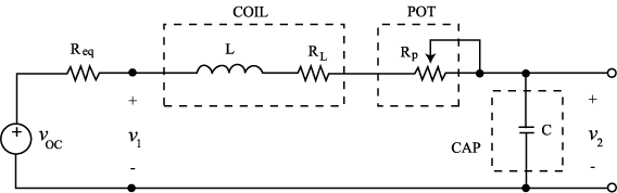
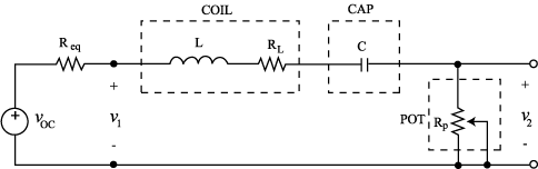
ĀĀĀ ĀĀĀĀĀĀĀĀĀĀĀ By Thevenin’s theorem, the circuit reduces to the equivalent of Fig. 5 for the case in which we want to observe the response across the capacitor.ĀĀ Here vOC and Reqare the parameters of the equivalent source, RL is the winding resistance of the coil, and Rp is a variable resistance to adjust the value of z (or Q) for our circuit.Ā This resistance is implemented by tying the wiper to one of the sides of the potentiometer.ĀĀ If you need a value of Rp greater than the potentiometer’s rating, use a suitable resistance in series.Ā The expressions for z and Q derived above still hold, provided we use
In our case, ReqĀ @ (50 + 100)//10 @ 9.4 W.
Initial Measurements and Calculations: Henceforth, steps shall be identified by letters as follows: C for calculations, M for measurements,Ā S for SPICE simulation. M1: Using an RLC meter from the stockroom, measure C, L, and RL.Ā Henceforth, each measured value should be expressed in the form X▒DX ( e.g. C = 10 nF ▒ 0.05 nF), where DX represents the estimated uncertainty of your measurement, something you have to figure out based on your learning in ENGR 300.Ā C2: Calculate the undamped natural frequency Step Response: While monitoring v1 with Ch.1 of the oscilloscope set on DC, adjust the signal generator so that v1 isĀ a square wave alternating between 0 V and 0.1 V with aĀ period of about 10/f0, where f0 is the undamped frequency of Step C2.Ā Make sure you know where the 0-V baseline is on the screen! C3:Ā Find the three values of R, and, hence, of Rp, that result in z = 1,z = 5, and z = 0.2.Ā For the case zĀ = 0.2, compute also the damped frequency fnand overshoot OS. C4:ĀĀ Calculate the values of the poles for the three specified values z, and show their complex plane locations.Ā Be neat and precise. S5: ĀUsing PSpice, along with the component values of Steps M1 and C3, plot the response of the circuit of Fig. 5 to a 0.1-V step for the three specified values of z .Ā For the case zĀ = 0.2,Ā use the cursor facility of PSpice to estimate the overshoot OS as well as the period Tn of the decaying oscillation and, hence, the damped frequency fn = 1/Tn.Ā Compare with the predicted values in Step C3, comment.ĀĀ M6:Ā Adjust Rp for z = 1; then, observe and record the circuit’s response by monitoring v2Ā with Ch. 2 of the oscilloscope set on DC.Ā Compare with the response predicted via PSpice in Step S5, and account for any discrepancies.Ā M7:Ā Repeat step M6 for the case z = 5.Ā Provide a physical justification for why the response is now so sluggish.Ā M8:Ā Repeat step M6 for the case z = 0.2.Ā Also, from the oscilloscope trace, estimate fn and OS Āin a manner similar to Step S5, compare with those predicted in Step C3, and comment.Ā Finally, provide a physical justification for why the response is now oscillatory.ĀĀĀ Impulse Response: Leaving the potentiometer setting as in Step M8, interchange RpĀ and C so that the circuit becomes as in Fig. 6.Ā Then, change the signal generator settings so that v1 is now a pulse train consisting of pulses alternating between 0 V and 0.1 V, with pulsewidth of about 1/10f0 and period of about 10/f0 , where f0 is the undamped frequency of Step C2. M9:Ā Observe and record the response v2, which, given the above characteristics of v1, can be regarded as a good approximation to the impulse response of the circuit.Ā Explain why, and use physical reasoning to justify the waveform of v2 .Ā Also, measure the frequency of oscillation and compare with its expected value. Frequency Response: To investigate this type of response, change the signal generator settings so that v1 is now a sinusoidal signal with an amplitude of 0.1 V, 0 V DC, and variable frequency f.Ā You can measure fĀ by (a) reading the settings of the frequency dial on the signal generator, or (b) by measuring the period TĀ with the oscilloscope and then computingĀ f = 1/T, or (c) by using a frequency meter from the stockroom.Ā It is up to each group to decide which method to
pursue, and to justify your choice in the final report.Ā No matter what method is chosen, frequency readings shall always be expressed in the form f▒Df , as per ENGR 300.Ā C10:Ā Find the value of R , and, hence, of Rp, that results in Q = 5.Ā Then, calculate fL, fH, and the bandwidth BW. S11: ĀUsing PSpice, along with the component values of Steps M1 and C10, generate the Bode Plots of the circuit of Fig. 6.Ā Then, using the cursor facility of PSpice, estimate fL andĀ fHĀ first as the –3-dB frequencies on the magnitude plot, then as the ▒45o frequencies on the phase plot.Ā Compare the resulting values of fL,Ā fH, and BW against those of Step C10, and account for possible discrepancies.Ā M12:Ā Vary the signal generator’s frequency fĀuntil v2 Āreaches its maximum.Ā This gives the experimental value of f 0, which you must express in the form f 0▒Df 0, as usual.Ā Compare with the calculated value of Step C2, and account for possible discrepancies.Ā Also, how does the maximum amplitude of v2 compare with the amplitude of v1?Ā Justify via suitable calculations! M13:Ā Vary the signal generator’s frequency f until the amplitude of v2 Āis down to 70.7% of itsĀ maximum as found in Step M12.Ā There are two such frequencies, namely,Ā fL andĀ fH, which must be expressed as fL▒DfL andĀ fH ▒DfH, as usual.Ā Compare with the calculated values of Step C10.Ā M14:Ā Repeat Step M13, except that you will now find fL andĀ fH as the ▒45o frequencies.Ā For phase measurements, refer to ENGR 206.Ā Which of the four above methods of estimating fL andĀ fH do you thinkĀ is the most dependable, and why?Ā Which the least dependable, and why?Ā M15:Ā Verify experimentally that for fĀ << f 0, increasing fĀ by a factor of 10 increases amplitude also by a factor of 10, this being the reason why it is said that the slope of the magnitude curve is +20 dB/dec there.Ā Likewise, verify experimentally that for fĀ >> f 0, increasing f by a factor of 10 decreases amplitude also by a factor of 10, this being the reason why the slope of the magnitude curve is said to beĀ – 20 dB/dec there.Ā M16:Ā Interchange RpĀ and C so that we are back to the circuit of Fig. 5 to observe the response across C. Find the value of R that results in Q= 1//2, and hence adjust Rp accordingly.Ā Then, by suitably varying the signal generator’s frequency f Āwhile leaving amplitude and DC offset unchanged, perform the following measurements:Ā (a) find the –3-dB frequency f-3dB, (b) find the low frequency amplitude of v2,Ā and (c) find the amplitude of v2 at 10f-3dB and 100f-3dB. C17:Ā Using the data of Step M16, construct the magnitude Bode plot of the response across the capacitor.Ā Hence, justify the designation second order low pass response.Ā What is the slope for fĀ >> f 0, in dB/dec? S18:ĀĀ Using PSpice, plot the magnitude response across C.Ā Then, compare with the plot of Step C17, and account for possible discrepancies.Ā |
||||||||||||||||||||||||||||||||||||||||||||