| Download lab in PDF format - |
|
ENGR 301 – Electrical Measurements Experiment # 4:Ā BJT Characteristics and Applications Objective:ĀĀ To characterize a bipolar junction transistor (BJT).Ā To investigate basic BJT amplifiers and current sources.Ā To compare measured and simulated BJT circuits.Ā Components:Ā 2 x 2N2222A npn BJTs, 2 x 2N3906 pnp BJTs, 1 x 1N4733 5.1 V, 1 W zener diode, 2 x 0.1 mF capacitors, 1 x 100 mF capacitor, 1 x 10 kW potentiometer, and miscellaneous resistors:Ā 1 x 100 W, 1 x 1.0 kW, 1 x 2.0 kW, 1 x 3.0 kW, 4 x 10 kW,Ā and 1 x 100 kW (all 1%, ╝ W).Ā Instrumentation:Ā A curve tracer, a bench power supply, a signal generator (sine/triangle wave), a digital multimeter, and a dual-trace oscilloscope.Ā References:Ā
Theoretical Background:Ā When a low-power npn BJT is biased in the forward-active region, defined by by the conditions
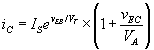
its collector current iCĀ is related to the applied base-emitter voltage drop vBE and the operating collector-emitter voltage vCE as
where IS , a current scale factor, is called the collector saturation current; VT, a voltage scale factor, is called the thermal voltage; VA, another voltage scale factor, is called the Early voltage.Ā At room temperature, VT @ 26 mVand IS is typically on the order of fAs for a low-power BJT.Ā Moreover, a low-power npn BJT typically exhibits VBE(on) @ 0.7 V and VCE(sat) @ 0.1 V; finally, VA is on the order of 102 V.Ā Note that the extrapolated value of iC in the limit vCE « 0 is iC = IS [exp (vBE /VT)].Ā A given pair of values IC Āand VCE in the iC -vCE plane define a unique point called the operating point Q(IC ,VCE) of the BJT. Similar considerations hold for pnp BJTs, provided we reverse all current directions and voltage polarities.Ā Thus, while in an npn BJT iCĀ and iB flow into and iE flows out of the device, in a pnp BJT iCĀ and iB flow out of and iE flows into the device.Ā Moreover, the forward-active conditions of Eq. (1) become, for a pnp BJT,
Similarly, Eq. (2) is rephrased as
The terminal currents of a forward-biased npn and pnp BJT are related as
where
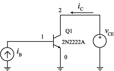
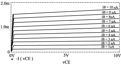
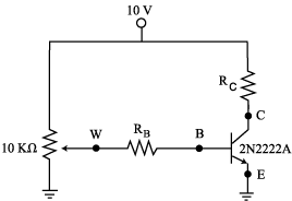
Typically, aF is very close to unity (e.g. aF Ā= 0.99), and bF is on the order of 102. BJT circuits are readily simulated using PSpice.Ā The file Eval.lib that comes with the student version of PSpice contains models for popular BJTs, including the 2N2222A npn and the 2N3906 pnp BJT.Ā For instance, to invoke a 2N2222A BJT from the built in library, we use a command of the typeĀ QXXX C B E Q2N2222A where QXXX is the name of the specific BJT, such as Q1, and C, B, and E are the collector, base, and emitter nodes, in that specific order.Ā Shown below is the PSpice code for the curve tracer circuit of Fig. 1, which is used to display the iC -vCE characteristics of a 2N2222A BJT called Q1: BJT Characteristics The characteristics are shown in Fig. 2.Ā
The following PSpice code is used to simulate the basic CE amplifier of Fig. 3: CE Amplifier After running PSpice, we obtain an output file with the following information: BIAS SOLUTION:ĀĀĀĀĀĀ NODEĀĀĀ VOLTAGEĀĀĀ NODEĀĀĀ VOLTAGEĀĀĀ NODEĀĀĀ VOLTAGEĀ NODEĀĀĀ VOLTAGEĀĀĀ NODEĀĀĀ VOLTAGEĀĀĀ NODEĀĀĀ VOLTAGE AC ANALYSIS: FREQĀĀĀĀĀĀĀ VM(1)ĀĀĀĀĀĀ VP(1)ĀĀĀĀĀĀ VM(6)ĀĀĀĀĀĀ
VP(6)ĀĀĀĀ We readily find the gain of this amplifier to be vo/vs = VM(6)/VM(1) = -93.51 V/V, = -0.9351/0.01 where the negative sign is implied by the fact that VP(6) @ -180o.ĀĀ You may find it instructive to confirm the above data (both bias and ac) via hand calculations! Curve Tracers: The iC -vCE characteristics of BJTs can be displayed experimentally on a cathode ray tube (CRT) by means of an instrument called curve tracer.Ā An example of such an instrument is the Tektronix Type 575 Transistor Curve Tracer available in our lab.ĀĀ Use the following steps to calibrate the instrument for displaying the iC -vCE characteristics of a 2N2222A npn BJT:Ā
Henceforth, steps shall be identified by letters as follows: C for calculations, M for measurements, and S for SPICE simulation.Ā Moreover, each measured value should be expressed in the form X▒DX ( e.g. bF = 125▒ 1), where DX represents the estimated uncertainty of your measurement, something you have to figure out based on your learnings in ENGR 300.Ā Forward-Active Characteristics: The PSpice model used in the above examples is based on typical 2N2222A parameter values as reported in the data sheets.Ā An actual BJT sample exhibits its own set of parameters, and we will measure some of them to gain an idea of its departure from typical data.Ā
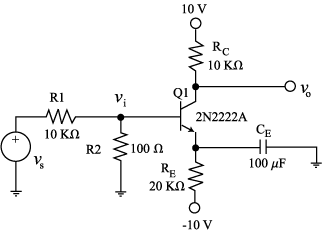
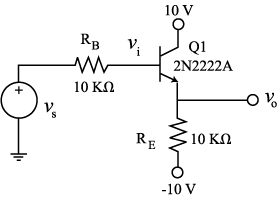
M1:Ā Mark one of your 2N2222A BJTs, and use the curve tracer to measure bF Āand ro at the operating point Q(IC , VCE ) = Q(1 mA, 5 V).Ā Recall that bFĀ = IC /IB, where IB is the base current required to sustain the desired IC , and that 1/ro is the slope of the iC -vCE curve at Q.Ā Then, estimate the Early voltage VA from 1/ro = IC/(VA + VCE).Ā Don’t forget to express your data in the form X▒DX.Ā Note: If the curve tracer is already in use by another group, proceed with the next steps and return to the present one later. M2:Ā With power off, assemble the circuit of Fig. 4 with RC = 5.0 kW (use 2 x 10-kW resistors in parallel) and RB = 500 kW (use 2 x 1.0-MW resistors in parallel); keep the leads short, and bypass the power supply bus with a 0.1-mF capacitor, as recommended in Appendix A2.Ā Then, apply power and adjust the potentiometer until VCE @ 5 V; record also the voltages VW Āand VBE (when measuring VBE, use as many digits as your DVM will allow). M3:Ā Turn power off, configure your DMM as a DC ammeter, break the circuit at node C, and insert the ammeter in series; then, reapply power and measure IC both with RC in place, as shown, and with RC shorted out with a wire.Ā The difference DIC between the two readings will be small, so make sure you use as many digits as your ammeter will allow.Ā Note that shorting out RC is designed to cause a change DVCE = 5 V. C4:Ā Use the data of Steps M2 and M3 to compute bF, VA, and IS at the operating point Q(1 mA, 5 V) as follows: (a) bFĀ = IC /IB, where IB is found as IB = (VW - VBE)/RB.Ā You may want to measure also RB for more accurate results (don’t forget to pull RB out of the circuit when measuring it!) (b) VA = roICĀ - VCE, where ro = DVCE /DICĀ (c) Don’t forget to express your data in the form X▒DX.Ā Then, compare the values of bF and VA withĀĀĀ those of Step M1, and comment.Ā Which set of values do you think is more dependable? Saturation Characteristics: To observe these characteristics we use again the circuit of Fig. 4, but with RC = 10 kW and RB = 100 kW.Ā As you make these changes, don’t forget to turn power off! M5:Ā Starting with the wiper voltage vW at zero, gradually rise vW while monitoring vCE with the DVM. As vW rises, vCE decreases until it saturates at vCE = VCE(sat).Ā Record the values of vW , vBE, and vCE at the point when vCE just begins to saturate, a situation aptly referred to as the edge-of-saturation.Ā Use the above data to calculate the ratio IC/IB at the edge of saturation; how does this ratio compare with the value of bF found earlier? M6:Ā Now rise the wiper all the way up to 10 V, while still monitoring vCE with the DVM.Ā Does vCE Āchange appreciably as the operating point is moved from edge-of-saturation to deep saturation?Ā What is the value of the ratio IC/IB when vWĀ = 10 V?Ā How does it compare with bF ?Ā Justify the designation bforced for the ratio IC/IB when operation is past the edge-of-saturation.ĀĀĀ Common-Emitter Amplifier: With power off, assemble the circuit of Fig. 5 (implement RE with 2 x 10-kW resistors in series), keeping the leads short and bypassing the power supply busses with 0.1-mF capacitors, as recommended in Appendix A2.Ā Since the input vi must be a small signal in order for the BJT to operate approximately linearly, we interpose a voltage divider R1 and R2 between the input source and the BJT to suitably scale down the source.Ā With the resistor values shown we have vi @ vs/100. C7:Ā Assuming vs has DC value of 0 V in Fig. 5, predict the DC voltages VB, VE, and VC at the base, emitter, and collector terminals, as well as the small signal gain Av = vo/vi.Ā M8:Ā While monitoring vs with Ch.1 of the oscilloscope (DC mode, Trigger from Ch. 1), adjust the signal generator so that vs in Fig. 5 is a 10-kHz sinewave with 0-V DC and 1-V peak amplitude (this makes vi a 10-mV peak amplitude sinewave).Ā Next, use CH. 2 (DC mode, Chop Mode), to measure the DC voltages at the base, collector, and emitter pins; finally, switch Ch. 2 to the AC mode and measure the peak amplitude of vo; hence, find the gain Av = vo/viof your amplifier.Ā
S9:Ā Simulate the circuit of Fig. 5 using PSpice.Ā For an effective simulation, you need to create a PSpice model for your specific BJT sample, .model our_BJT npn (IS=Ival BF=Bval VAF=Vval) where Ival, Bval,and Vval are the (most dependable) values of IS, bF, and VA as found experimentally above.Ā To invoke your transistor, you then use a command of the type:Ā QXXX C B E our_BJT. C10:Ā Compare the predicted values of Step C7 with the measured values of Step M8 and the simulated values of Step S9;Ā account for possible discrepancies.Ā
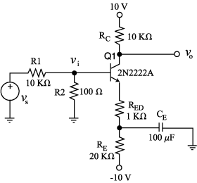
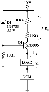
M11:Ā Returning to the circuit of Fig.5, switch Ch. 2 back to the DC mode (make sure you know where your 0-V baseline is on the screen!), change the input generator’s waveform from sinusoidal to triangular, and rise its amplitude until vo first begins to distort, then until it clips both at the top and at the bottom (in case the generator’s maximum amplitude is not large enough, you my have to remove R2 from your circuit).Ā What causes distortion to occur?Ā What are the values of the upper and lower clipping voltages?ĀĀ Justify the two clippings in terms of transistor operation.Ā CMS12:Ā With poweroff, insert a 1-kW emitter degeneration resistor as shown in Fig. 6.Ā Then, repeat Steps C7, M8, S9, and C10 for this new circuit.Ā Hence, justify and verify the following well known rule of thumb: the gain of a CE amplifier with emitter degeneration is Av @ RC/RED. Common-Collector Amplifier: With power off, assemble the circuit of Fig. 7, keeping leads short and using 0.1-mF power supply bypass capacitors, as usual.Ā Then, adjust the input source so that vs is a 10-kHz sinewave with 0-V DC and 5-V of peak-to-peak amplitude.Ā CMS13:Ā Assumingvs has DC value of 0 V in Fig. 7, predict the DC voltages VB and VE, as well the small signal gain Av = vo/vi.Ā Next, measure VB, VE, and Av.Ā Next, find VB, VE, and Av via PSpice.Ā Finally, compare the three sets of values, and account for possible discrepancies.Ā Note:Ā In this circuit, vs has 5-V peak-to-peak amplitude, hardly a small signal; show that the BJT is nevertheless still operating under small signal conditions! M14:Ā In the circuit of Fig. 7 connect a load resistance RL = 10 kW between the output and ground.Ā Is the amplitude of vo affected appreciably?Ā Justify your findings!Ā Next, with RL in place, increase the amplitude of vs (while leaving its DC value at 0 V) until vo begins to clip at the bottom.Ā At what voltage level does vo clip?Ā What causes this clipping to occur?Ā Hint:Ā What happens to vo if you remove RL from your circuit? Current Source:Ā One of the most popular applications of BJTs is as current sources (pnp BJTs) or current sinks (npn BJTs); in either case the output current is the collector current, thanks to the high resistance presented by this terminal.Ā In the current source example of Fig. 8, D1 establishes a reference voltage for biasing the BJT, and RE establishes the output current as IOĀ = (VZ Ā- VEB(on))/RE
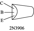
MC15:Ā Mark one of your 2N3906 BJTs, and use the curve tracer to estimate its Early voltage VA.Ā Note: The estimation of VA is similar to that of Step M1, except that you now need to adjust the POSITION knobs so that the origin of the i-v characteristic is at the upper right corner of the CRT; moreover, you must switch the POLARITY knobs from + to - both in the BASE STEP GENERATOR and the COLLECTOR SWEEP controls.Ā Once you have VA, estimate the output resistance Ro of the current source of Fig. 8 as seen by the load; do your estimation for for the case IO = 1.0 mA M16:Ā With power off, assemble the circuit of Fig. 8, keeping leads short and using a 0.1-mF power supply bypass capacitor, as usual.Ā Then, with the multimeter configured as a digital current meter (DCM) and using first a wire as a load, turn on power and adjust the pot for IO = 1.0 mA.Ā Next, turn power off, insert a 3.0-kW load, and turn again power on: does IO change appreciably in spite of the 3-V change in the load voltage VL?Ā Justify in terms of the output resistance Ro estimated in Step. MC15. MC17:ĀĀ Now rise the supply voltage from 10 V to 15 V while monitoring IO with the DCM.Ā By how much does IO change?Ā Justify quantitatively in terms of the zener diode model!
|
|||||||||||||||||||||||||||||||||||||||